Wafer bonding with highly compliant plate having filler material enclosed hollow core

a technology of compliant plate and filler material, which is applied in the direction of basic electric elements, electrical equipment, semiconductor devices, etc., can solve the problems of increasing the power consumption of the device on the chip, slowing down the speed, and damage to the taller contacts

Active Publication Date: 2007-12-11
TAHOE RES LTD
View PDF8 Cites 222 Cited by
  • Summary
  • Abstract
  • Description
  • Claims
  • Application Information

AI Technical Summary

Problems solved by technology

As the smallest CD that may be achieved for the feature has been inexorably decreased, the fundamental limitations of physics will inevitably slow down the speed and increase the power consumption of the devices on the chip.
In another case, shorter contacts may bond, but taller contacts may be damaged.

Method used


Image

  • Wafer bonding with highly compliant plate having filler material enclosed hollow core
  • Wafer bonding with highly compliant plate having filler material enclosed hollow core
  • Wafer bonding with highly compliant plate having filler material enclosed hollow core

Examples


Embodiment Construction

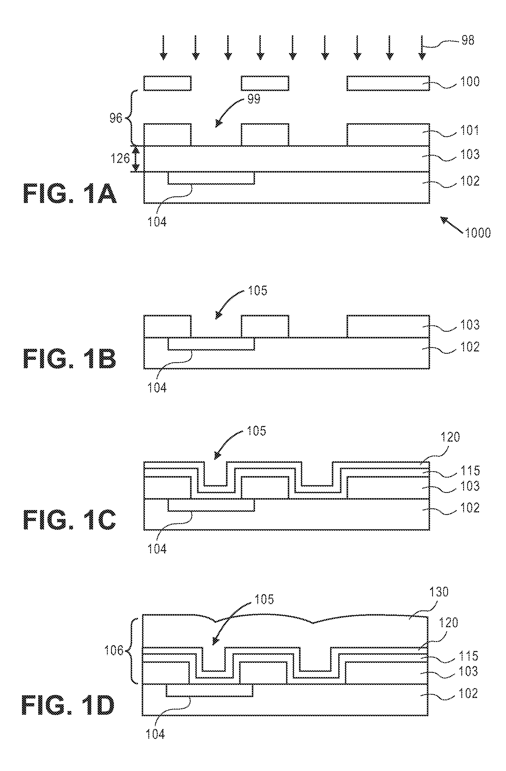
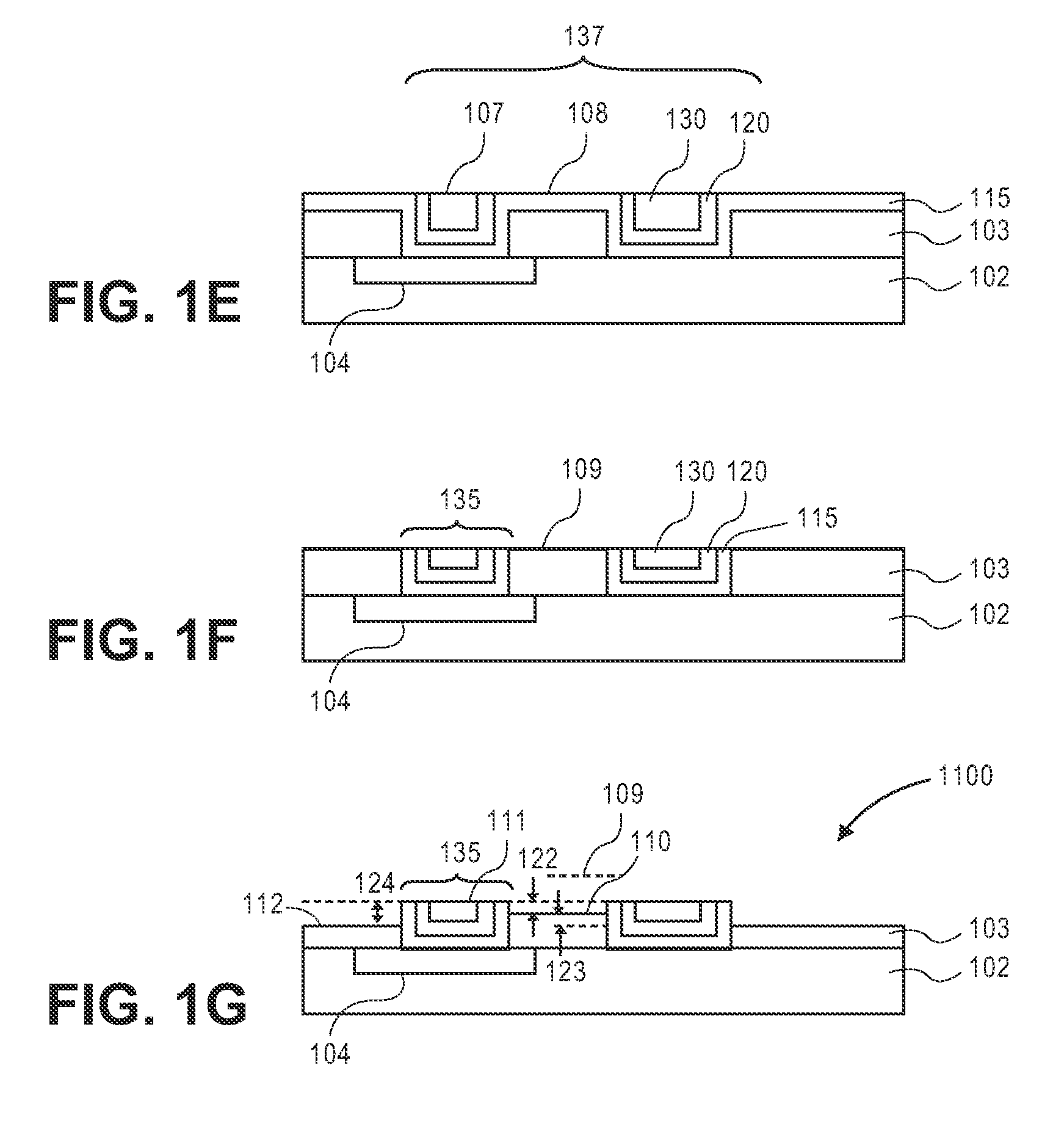
[0012]In the following description, numerous details, such as specific materials, dimensions, and processes, are set forth in order to provide a thorough understanding of the present invention. However, one skilled in the art will realize that the invention may be practiced without these particular details. In other instances, well-known semiconductor equipment and processes have not been described in particular detail so as to avoid obscuring the present invention.

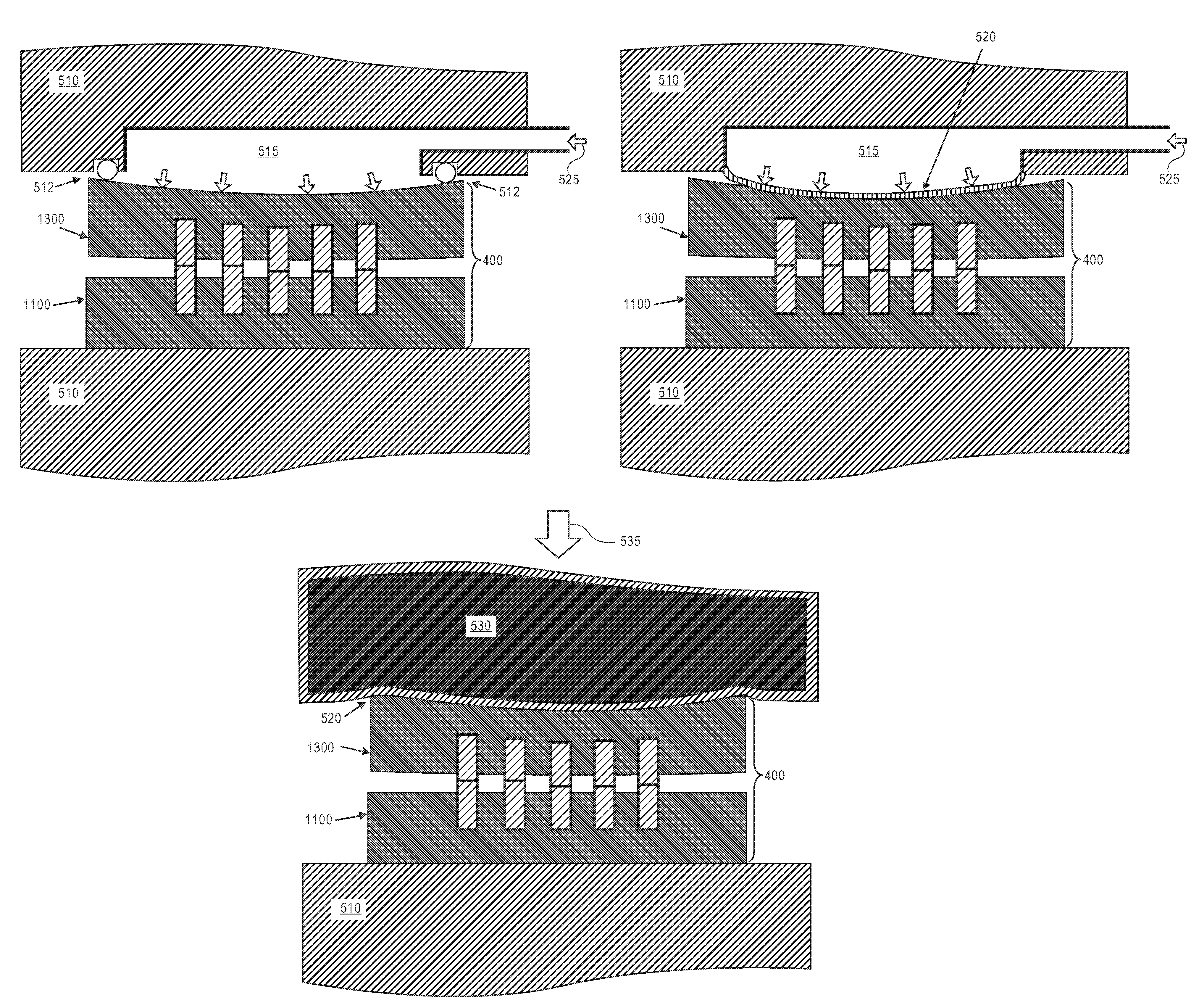
[0013]Various embodiments of a method of bonding wafers using highly compliant plates will be described first, followed by various embodiments of a bonded-wafer structure having copper contacts with variable heights. In an embodiment of the present invention, the wafers being bonded may be similar with respect to materials, structures, dimensions, or functions. In another embodiment of the present invention, the wafers being bonded may be dissimilar in one or more respects.

[0014]The wafers may have an initial thickness se...


PUM


Abstract

The present invention discloses a method that includes: providing two wafers; forming raised contacts on the two wafers; aligning the two wafers; bringing together the raised contacts; locally deflecting the two wafers; and bonding the raised contacts.The present invention also discloses a bonded-wafer structure that includes: a first wafer, the first wafer being locally deflected, the first wafer including a first raised contact; and a second wafer, the second wafer being locally deflected, the second wafer including a second raised contact, wherein the second raised contact is bonded to the first raised contact.

Description

BACKGROUND OF THE INVENTION[0001]1. Field of the Invention[0002]The present invention relates to the field of semiconductor integrated circuit (IC) manufacturing, and more specifically, to a method of bonding wafers using highly compliant plates, as well as, a bonded-wafer structure having copper contacts with variable heights.[0003]2. Discussion of Related Art[0004]In 1965, Gordon Moore first observed that the maximum number of devices per area on a chip was doubling every 18 months. Over the four decades since Moore's Law was first stated, the semiconductor industry has successfully introduced new processes and designs to maintain such a rate of increasing device density. In particular, continual enhancements in photolithography have reduced the minimum critical dimension (CD) that may be successfully patterned for a feature on the devices on the chip. Furthermore, major developments in doping, deposition, and etch have allowed a greater precision in controlling concentration, dep...

Claims


Application Information

Patent Timeline
Patent Type & Authority Patents(United States)
IPC IPC(8): H01L21/30
CPCH01L21/76885H01L2224/05181H01L2224/05186H01L2924/04953H01L2924/00014
Inventor KOBRINSKY, MAURO J.RAMANATHAN, SHRIRAMLIST, SCOTT RICHARD
Owner TAHOE RES LTD
Why Eureka
Try Eureka