Methods for forming a ferroelectric layer and capacitor and FRAM using the same

a technology of ferroelectric layer and capacitor, which is applied in the direction of coating, chemical vapor deposition coating, coating process, etc., can solve the problems of increasing the probability of causing misalignment, complex fabrication of recessed ir barrier, and inability to manufacture conventional fram devices, etc., to achieve the effect of improving the uniformity of the resulting layer

Active Publication Date: 2007-12-25
SAMSUNG ELECTRONICS CO LTD
View PDF3 Cites 8 Cited by
  • Summary
  • Abstract
  • Description
  • Claims
  • Application Information

AI Technical Summary

Benefits of technology

[0015]In exemplary embodiments of the present invention, methods of forming a ferroelectric layer may utilize a metal organic vapor deposition (MOCVD). The MOCVD may include a process chamber for applying an MOCVD process to a substrate; a susceptor for heating the substrate to a reaction temperature of MOCVD; a showerhead; a first gas inflow device which may include a vaporizer and may guide the metal organic precursor gas to a first jet element; and a second gas inflow device which may include a heater and may guide the oxidizer gas to a second jet element. The showerhead may comprise the first jet element for spraying the metal organic precursor gas and the carrier gas, which may be in a heated state into the process chamber; and the second jet element for spraying the oxidizer gas, which may be in a heated state, into the process chamber. The showerhead may suppress a pre-mixing of the heated metal organic precursor gas and the heated oxidizer gas before passing the first and second jet elements.
[0016]In exemplary embodiments of the present invention, a distance between the showerhead 520 and the wafer 100 may be controllable to improve the uniformity of the resulting layer which may be at least one of an oxide, nitride, and carbide layer.
[0028]The showerhead may comprise: the first jet element which may spray the metal organic precursor gas and the carrier gas, which may be in a heated state, into the process chamber; and the second jet element which may spray the oxidizer gas, which may be in a heated state, into the process chamber. The showerhead may suppress a pre-mixing of the heated metal organic precursor gas and the heated oxidizer gas before passing through the first and second jet elements.

Problems solved by technology

However, the conventional FRAM devices may not be fabricated such that they may be used in the SoCs.
Fabrication of the recessed Ir barrier may be complex because it may utilize an Ir deposition, etching, and / or chemical mechanical polishing (CMP) processes.
As the capacitor area may decrease, which may be a result of an increase of a device integration density, the probability of causing misalignment may increase during photolithographic processes which may be used to form the recessed Ir barrier and the lower electrode.
The (111) oriented PZT may utilize a higher temperature (for example, 620° C.) to be deposited, and therefore the process temperature of the MOCVD may be increased to deposit the PZT, such that structural and / or operational problems may arise due to the higher temperature.

Method used


Image

  • Methods for forming a ferroelectric layer and capacitor and FRAM using the same
  • Methods for forming a ferroelectric layer and capacitor and FRAM using the same
  • Methods for forming a ferroelectric layer and capacitor and FRAM using the same

Examples


Embodiment Construction

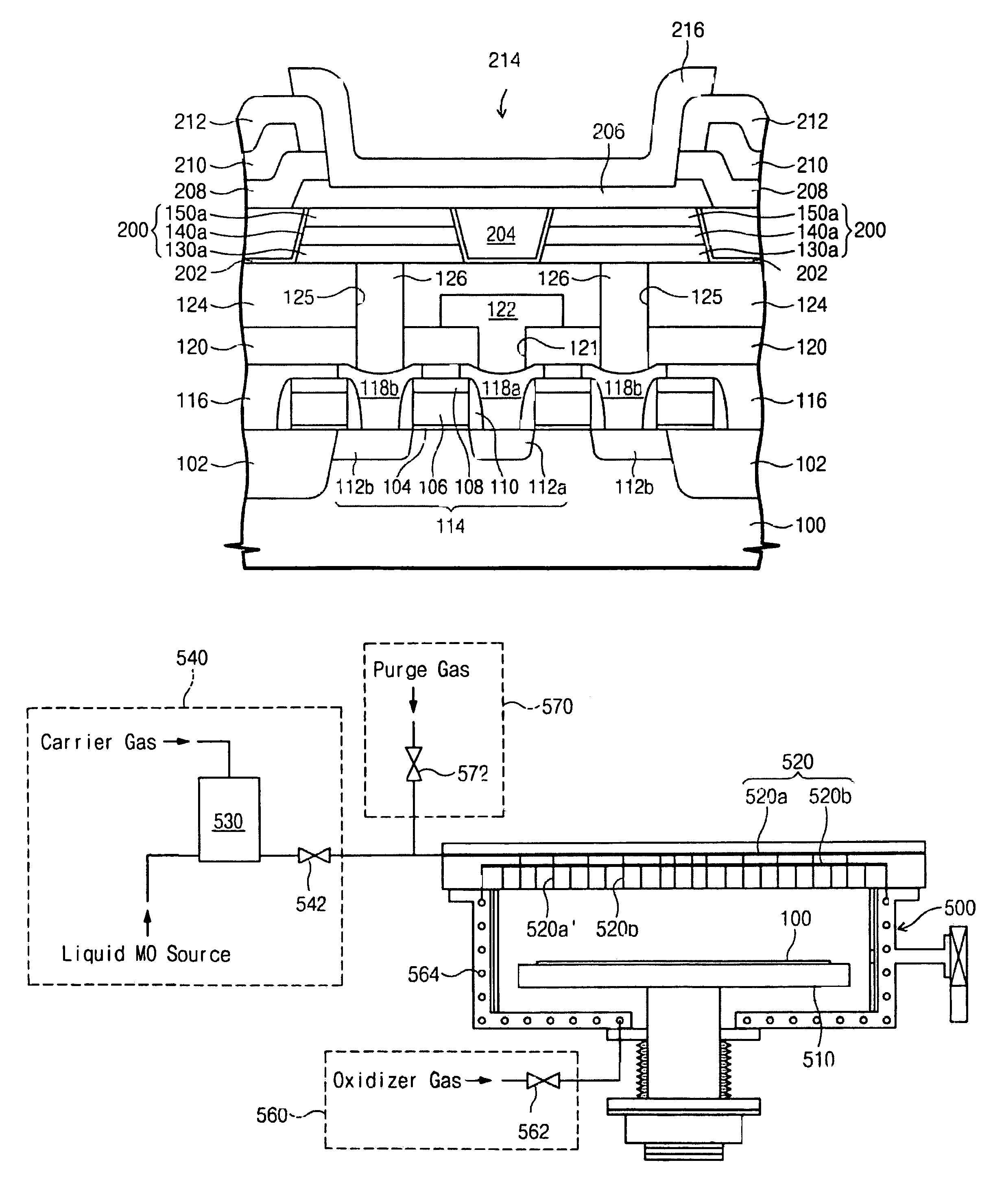
[0050]The present invention will be described more fully with reference to the accompanying drawings, in which exemplary embodiments of the invention are shown. It should be understood, however, that exemplary embodiments of the present invention described herein can be modified in form and detail without departing from the spirit and scope of the invention. Accordingly, the exemplary embodiments described herein are provided by way of example and not of limitation, and the scope of the present invention is not restricted to the particular embodiments described herein.

[0051]In particular, the relative thicknesses and positioning of layers or regions may be reduced or exaggerated for clarity. Further, a layer is considered as being formed “on” another layer or a substrate when formed either directly on the referenced layer or the substrate or formed on other layers or patterns overlaying the referenced layer.

[0052]In an exemplary embodiment of the present invention, referring to FIG....


PUM

PropertyMeasurementUnit
reaction temperatureaaaaaaaaaa

Abstract

Metal organic chemical vapor deposition (MOCVD) may be utilized in methods of forming an (111) oriented PZT ferroelectric layer at a lower temperature, a ferroelectric capacitor and methods of fabricating, and a ferroelectric memory device using the same may be provided. Using the metal organic chemical vapor deposition, ferroelectric layers, capacitors, and memory devices, which may be fabricated and may have (111) preferred oriented crystal growth.

Description

PRIORITY STATEMENT[0001]This application is a continuation-in-part application of “Apparatus For Fabricating Semiconductor Devices, Heating Arrangement, Shower Head Arrangement, Method of Reducing Thermal Disturbance During Fabrication Of A Semiconductor Device, And Method Of Exchanging Heat During Fabrication Of A Semiconductor Device” by the present inventors, U.S. Ser. No. 10 / 784,772, filed on Feb. 24, 2004 and a continuation-in-part application of “Method And Apparatus For Forming A Ferroelectric Layer” by the present inventors, U.S. Ser. No. not yet assigned, filed concurrently herewith, the contents of both of which are hereby incorporated by reference in their entirety. This application also claims the benefit under 35 U.S.C. § 119(a) of Korean Patent Application No. 2003-0051434, filed on Jul. 25, 2003, the contents of which are hereby incorporated by reference in their entirety.FIELD OF THE INVENTION[0002]The present invention relates to a method and apparatus for forming a...

Claims


Application Information

Patent Timeline
Patent Type & Authority Patents(United States)
IPC IPC(8): H01L21/00C23C16/44C23C16/452C23C16/455
CPCC23C16/4411C23C16/45565C23C16/45514C23C16/452
Inventor LEE, MOON-SOOKBAE, BYOUNG-JAE
Owner SAMSUNG ELECTRONICS CO LTD
Why Eureka
Try Eureka