Circuit component mounting device

a technology of circuit components and mounting devices, which is applied in the incorporation of printed electric components, printed circuit aspects, and final product manufacturing, etc., can solve the problems of preventing higher integration, and achieve the effect of preventing electromagnetic field interference and preventing solder bridging

Inactive Publication Date: 2007-12-25
COLLABO INNOVATIONS INC
View PDF5 Cites 11 Cited by
  • Summary
  • Abstract
  • Description
  • Claims
  • Application Information

AI Technical Summary

Benefits of technology

[0008]The present invention has its object of providing a circuit component mounting device capable of preventing solder bridging and preventing electromagnetic field interference between a circuit component and a circuit pattern.
[0010]With the above structure, the region interposed between the two conductor members in the region between the substrate and the circuit component becomes easy to be filled with the insulator. This prevents the solder re-dissolved in reflow after the circuit component is mounted on the substrate from flowing into the space, whereby solder bridging that brings a short circuit between the conductor members can be prevented. Further, the increase in height of the circuit component suppresses variation in electric characteristics of the circuit component which is due to influence from the ground.
[0013]In the circuit component mounting device of the first aspect of the present invention, the conductor members may include balls formed by wire bonding. When the balls formed by wire bonding are used as the conductor members, the distance between the two conductor members can be shortened up to about 50 μm. Accordingly, the present invention becomes applicable to devices of which circuit component to be mounted is small, for example, in 0.4 mm×0.2 mm size. Especially, when a ceramic substrate, which necessitates firing, is used as the substrate, it is difficult to form a thick plate on the substrate. Hence, this method employing wire bonding becomes much effective.
[0014]In the circuit component mounting device of the first aspect of the present invention, a circuit pattern made of a conductive material may be formed on another part of the substrate. In this case, the distance between the circuit component and the circuit pattern becomes longer than that of the conventional one, reducing the electromagnetic field interference therebetween. In other words, this structure gains a vertical distance between the circuit component and the circuit pattern, so that a horizontal distance therebetween can be reduced compared with the conventional one. Hence, element compaction can be attained.
[0017]With this structure, the region interposed between the two conductor members in the region between the substrate and the circuit component becomes easy to be filled with the insulator. This prevents the solder re-dissolved in reflow after the circuit component is mounted on the substrate from flowing into the space. Whereby, the solder bridging that brings a short circuit between the conductor members can be prevented. Further, with the circuit component increased in height, variation in electric characteristics, which is due to influence from the ground, can be reduced.
[0018]Moreover, the distance between the circuit component and the circuit pattern becomes longer than that of the conventional one, reducing the electromagnetic field interference therebetween. In other words, this structure gains a vertical distance between the circuit component and the circuit pattern, so that a horizontal distance therebetween can be reduced compared with the conventional one. Hence, element compaction can be attained.

Problems solved by technology

However, this inhibits higher integration.

Method used


Image

  • Circuit component mounting device
  • Circuit component mounting device
  • Circuit component mounting device

Examples


embodiment 1

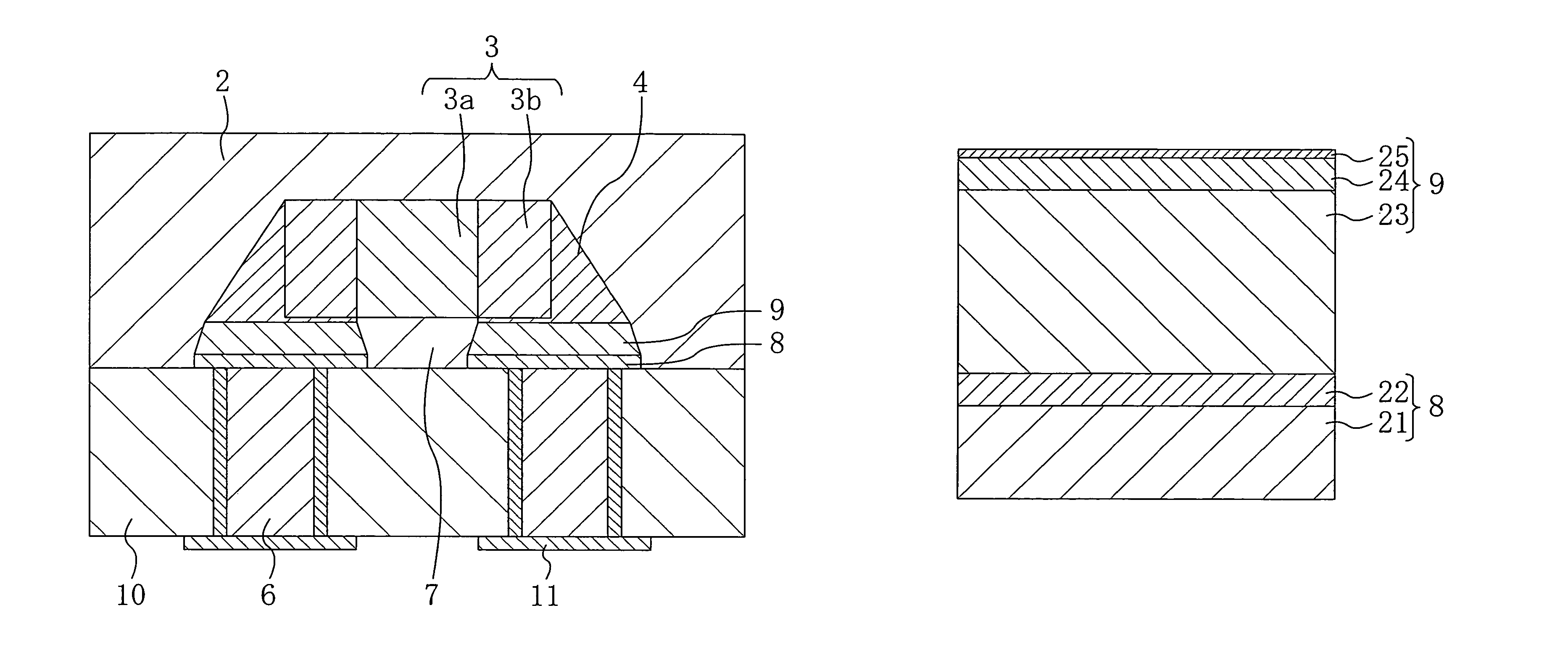
[0029]FIG. 1A is a section showing a structure of a circuit component mounting device of Embodiment 1. As shown in FIG. 1A, the circuit component mounting device of the present embodiment includes: a resin substrate (or a multilayered resin substrate) 10; vias 6 of which via holes passing through the resin substrate 10 are filled with a conductive resin; a base metal pattern 8 that covers a part of the principal face of the resin substrate 10 where the vias 6 are exposed; a copper plated pattern 9 provided on the base metal pattern 8; a circuit component 3 provided on the copper plated pattern 9 and composed of a main body 3a and electrode portions 3b; a solder 4 for allowing the copper plated pattern 9 and the circuit component 3 to adhere to each other; an insulative sealing resin 2 that covers the circuit component 3 and the solder 4; and electrodes 11 that cover parts of the reverse face of the resin substrate 10 where the via holes are expose. The circuit component 3 is in 0.6 ...

embodiment 2

[0037]FIG. 3 is a section showing a structure of a circuit component mounting device of Embodiment 2. As shown in FIG. 3, in the present embodiment, a ceramic substrate (or a multilayered ceramic substrate) 12 is used rather than the resin substrate 10 (shown in FIG. 1) used in Embodiment 1. On the ceramic substrate 12, there are provided a base metal pattern 8 formed by firing and having a thickness of about 15 μm and Au balls 13 formed on the base metal pattern 8 by wire bonding. The firing is performed at a temperature between about 800 and 1500° C. after applying a paste-state Cu film (now shown) and a paste-state Ni film (not shown). A circuit component 3 composed of a main body 3a and electrode portions 3b are arranged on the Au balls 13. The other constitution is the same as that of Embodiment 1, and the description thereof is omitted.

[0038]The Au balls 13 are formed by two-time wire bonding after the substrate in which the base metal pattern 8 has been formed is introduced i...

embodiment 3

[0042]FIG. 4 is a section showing a structure of a circuit component mounting device of Embodiment 3. As shown in FIG. 4, difference in the present embodiment from Embodiment 1 lies in that a GND pattern 14 is formed on the reverse face of the resin substrate 10. The other constitution is the same as that in Embodiment 1, and the description thereof is omitted.

[0043]In the structure in the present embodiment, the circuit component 3 is formed high from the upper level of the resin substrate 10, so that the circuit component 3 receives less influence of variations in conductivity and film thickness of the resin substrate 10. Whereby, the electric characteristics of the circuit component 3 vary less.

[0044]FIG. 5 is a graph showing the state in which inductor values of thin film coils vary with distance between the circuit component 3 and the resin substrate 10. In the graph of FIG. 5, the axis of abscissas indicates the height of the circuit component 3 from the resin substrate 10 whi...


PUM

PropertyMeasurementUnit
heightaaaaaaaaaa
thicknessaaaaaaaaaa
thicknessaaaaaaaaaa

Abstract

A circuit component mounting device includes a resin substrate, vias, a circuit component composed of a main body and electrode portions, a solder, and an insulative sealing resin that covers the circuit component and the solder. The device further includes a base metal pattern which covers parts of the principal face of the resin substrate where the vias are exposed and is composed of a Cu layer and a Ni layer and a copper plated pattern which is provided on the base metal pattern and is composed of a Cu layer, a Ni layer, and an Au layer. The circuit component is provided on the copper plated pattern. The solder allows the copper plated pattern and the circuit component to adhere to each other.

Description

BACKGROUND ART[0001]The present invention relates to a circuit component mounting device in which a circuit component is mounted on a substrate, and particularly relates to a structure of a circuit component mounting device in which conductor members provided on a substrate adhere to a circuit component by means of a solder.[0002]Recently, circuit component mounting devices are being developed in which a highly-integrated circuit component is mounted and the mainstream structure thereof employs a circuit component covered with an insulative sealing resin in view of cost merits such as efficient production and the like. The circuit component is mounted on a set substrate after being packaged using a solder as an adhesive. This solder is dissolved in reflow for mounting to involve solder bridging that brings a short circuit between electrodes of the circuit component. This phenomenon is such that a several-micron gap remaining between the circuit component and the surface of the subst...

Claims


Application Information

Patent Timeline
Patent Type & Authority Patents(United States)
IPC IPC(8): H05K1/16
CPCH05K1/111H05K3/284H05K3/3442H05K3/243H05K3/244H05K3/4015H05K2201/10636H05K2201/0341H05K2201/0347H05K2201/09481H05K2201/0959H05K2201/09736H05K2201/0209Y02P70/50
Inventor YAMAMOTO, KOUKI
Owner COLLABO INNOVATIONS INC
Why Eureka
Try Eureka