
Enhanced timing margin memory interface

a memory interface and timing margin technology, applied in logic circuits, digital storage, instruments, etc., can solve the problems of low yield production, low yield production, and high cost of memory modules

Inactive Publication Date: 2007-12-25
MASHHOON HAMID R
View PDF2 Cites 2 Cited by
  • Summary
  • Abstract
  • Description
  • Claims
  • Application Information

AI Technical Summary

Benefits of technology

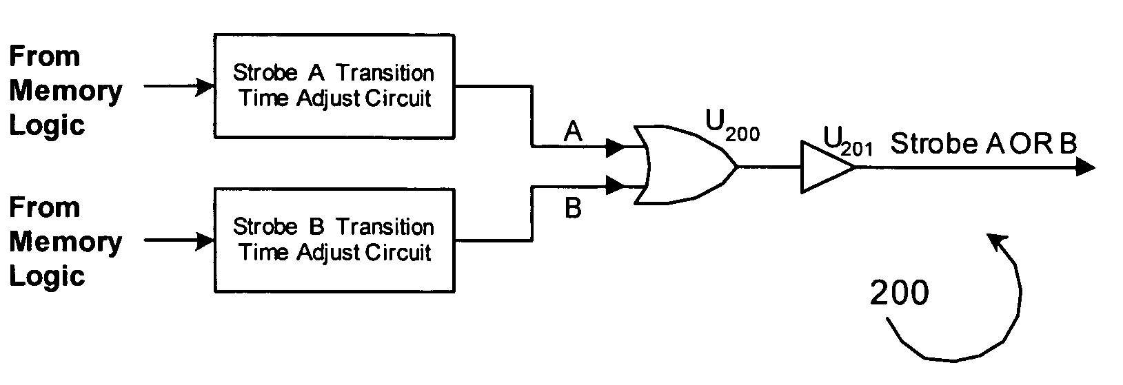
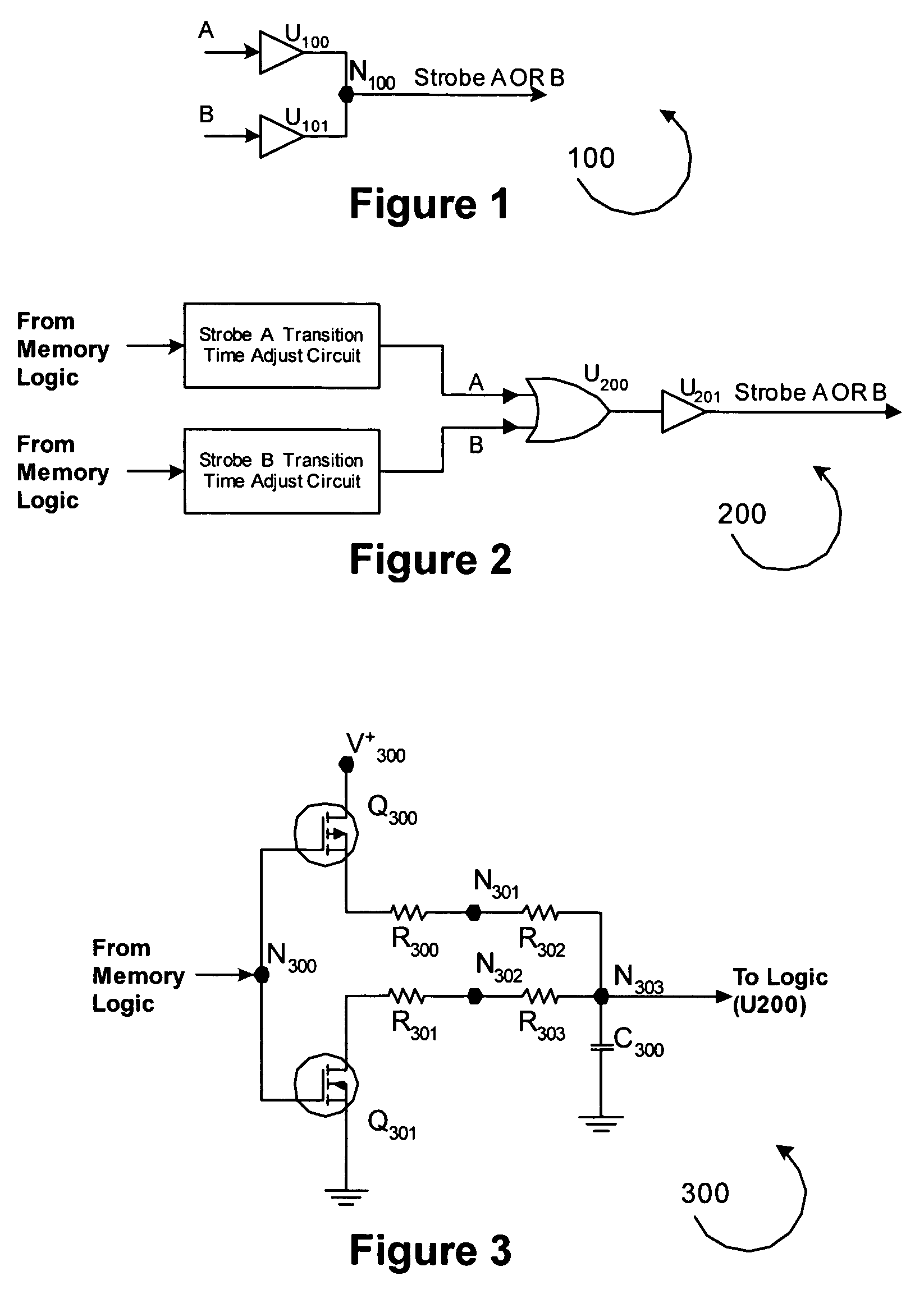
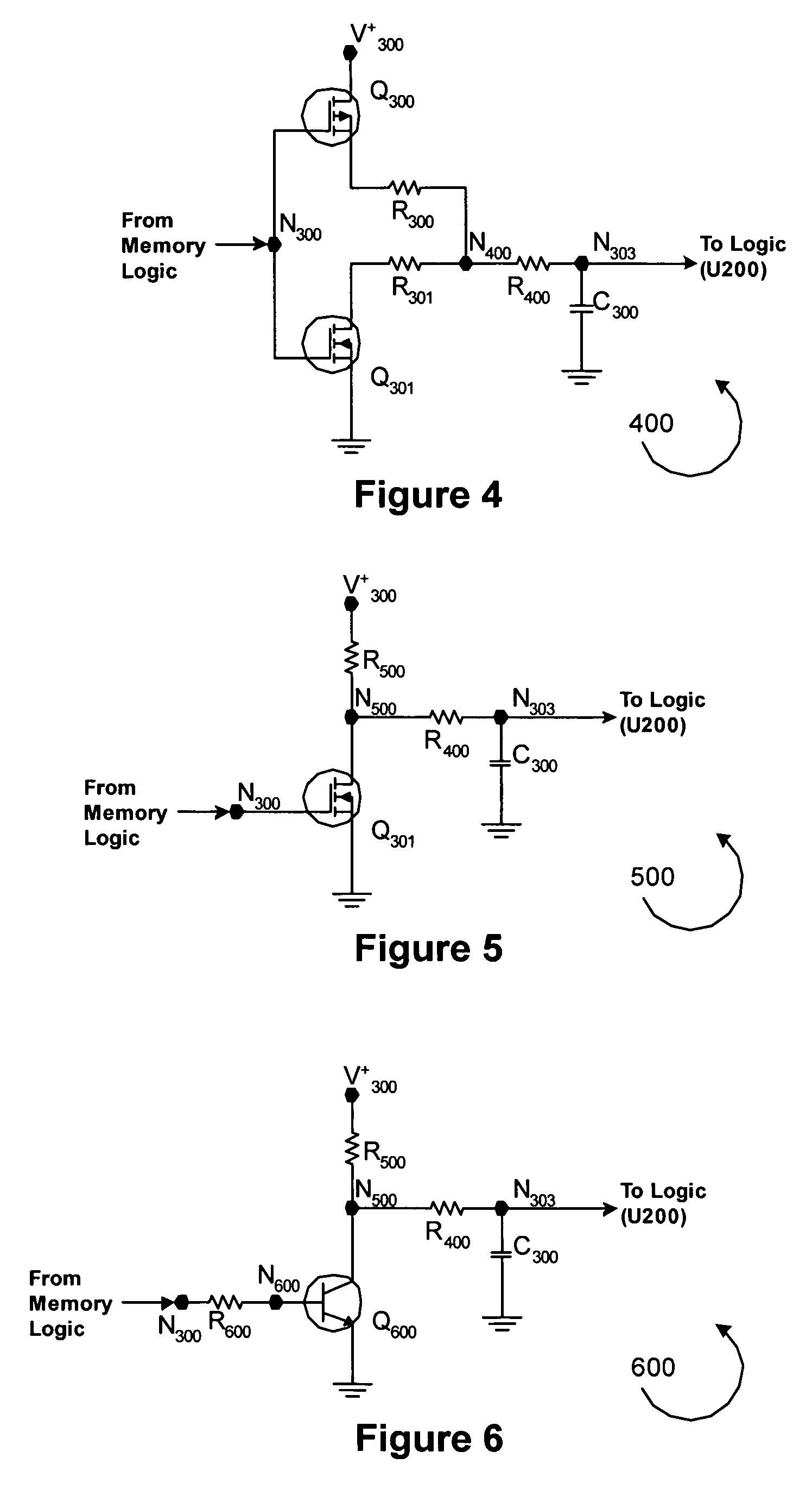
[0010]The present invention is an active, electronic circuit that is used within a digital memory circuit and comprises a number of features. One feature is the use of a single line driver per memory bus line instead of the wired-OR line drivers used in the present art. Another feature is the use of one or more logic gates to perform signal combining or signal selection functions and thereby avoid the need for the multiple, wired-OR line drivers used in the present art. Another feature comprises the use of timing margin enhancement circuits that independently adjust the rise and fall time of the digital signal transitions for each signal that would be applied to and drive the memory bus line through its separate line driver in the present art. The timing margin enhancement circuits are applied to both memory data and control / status signals.

Problems solved by technology

With the increasing need for higher speed memory, timing margin can no longer be ignored.
Since transition times and time delays are subject to manufacturing variability, timing margin has become both small and widely variable.
This makes for low yield production and very costly memory modules.
In addition to the timing margin problem, the trend has been toward larger and larger capacity memory modules.
The transition period with associated high current draw has resulted in a major power consumption / distribution problem for state of the art memory modules.
One of the major sources for high power consumption is the use of simple wired-OR connections of multiple line driver outputs driving the memory buss.
This results in high transient current flow and resulting high power dissipation.
At high memory clock rates, this represents a high “duty cycle” that will only become worse with increasing memory clock rates in the future.
For large memory modules, there are such a large number of the transitions occurring at a typical clocked transition that the total power consumption is large and difficult to deal with given conventional memory module to motherboard interfacing.

Method used


Image

  • Enhanced timing margin memory interface
  • Enhanced timing margin memory interface
  • Enhanced timing margin memory interface

Examples


Embodiment Construction

[0018]The present invention is directed to circuitry for use in a memory module. In the following description, numerous specific details are set forth to provide a more thorough description of embodiments of the invention. It is apparent, however, to one skilled in the art, that the invention may be practiced without these specific details. In other instances, well known features have not been described in detail so as not to obscure the invention. Except as noted herein, common components and connections, identified by common reference designators function in like manner in each circuit.

[0019]The present invention is illustrated in FIG. 2 and comprises a single line driver for the memory buss line being driven, one or more combinational logic gates for selecting or combining logic signals to be communicated over the memory buss line, and a transition time adjustment circuit for each signal that would other be wired-OR through its line driver buss interface in the present art. Strob...


PUM


Abstract

The present invention is an electronic circuit that significantly enhances timing margin in high-speed, digital memory modules. The circuit is implemented is applicable to all switching waveforms on both control and data signal lines that drive the memory bus. Implementation of the present invention also provides a significant reduction in power dissipation compared to memory modules of comparable size and speed utilizing the present art.

Description

CROSS-REFERENCE TO RELATED APPLICATION[0001]The present application claims the benefit of priority from pending U.S. Provisional Patent Application No. 60 / 602,548, entitled “Enhancing Timing Margin Memory Interface”, filed on Aug. 17, 2004, which is herein incorporated by reference in its entirety.BACKGROUND OF THE INVENTION[0002]1. Field of the Invention[0003]The present invention relates to the field of digital memory modules and more specifically it relates to means for transmitting data and control signals onto individual lines in the memory interface buss.[0004]2. Background Art[0005]Digital memory modules such as used in computers, printers, and telecommunications equipment are clocked devices that must communicate data, control, and status signals onto a memory buss. The signals are digital signals that are typically switched synchronously with the memory clock. Following a clocked transition, signals require a period of time to stabilize and allow switching transients to die...

Claims


Application Information

Patent Timeline
Patent Type & Authority Patents(United States)
IPC IPC(8): H03K19/0175
CPCG11C5/04G11C7/10G11C7/1066G11C7/1051G11C7/1048
Inventor WASHBURN, ROBERT D.MCCLANAHAN, ROBERT F.
Owner MASHHOON HAMID R
Learn More