Thin layer transfer method utilizing co-implantation to reduce blister formation and to surface roughness

a transfer method and co-implantation technology, applied in the direction of basic electric elements, electrical apparatus, semiconductor devices, etc., can solve the problems of voids appearing between the bonded substrates, increasing the risk of blister formation at the bonding interface, and increasing the risk of zones not being transferred onto the support substrate, so as to minimize the formation of blisters in the transfer layer and the surface roughness of the transfer layer

Active Publication Date: 2008-02-05
SOITEC SA
View PDF8 Cites 17 Cited by
  • Summary
  • Abstract
  • Description
  • Claims
  • Application Information

AI Technical Summary

Benefits of technology

[0026]The invention relates to a method for producing a semiconductor structure which comprises conducting controlled co-implanting of at least first and second different atomic species into a face of donor substrate to create an embrittlement zone which defines a thin layer of donor material to be transferred. This step is conducted by selecting implantation energies so that the coimplanting is made under conditions such that the first and second species are respectively distributed in the donor wafer according to a repartition profile that presents a spreading zone in which each species is mainly distributed and at a maximum concentration peak. Also, the implantation doses and implantation energies of the first and second species are selected such that the second species is implanted deeper in the embrittlement zone than the first species spreading zone, with the first species selected to provide essentially chemical implantation to thus form platelet defects in the donor substrate, and with the second species selected to provide physical implantation to thus act as a source of internal pressure in the donor wafer to impart stress upon the platelet defects. Next, the face of the donor substrate is placed into contact with a support substrate, and then the donor substrate is detached at the embrittlement zone to transfer the thin layer to the support substrate while minimizing blister formation in and surface roughness of the transferred layer. Preferably, the implantation dose of the first species is between about 40 to 60 percent and generally about 50% of all implantation doses. This method is preferably utilized for forming or producing SeOI (Semiconductor On Insulator) structures.

Problems solved by technology

However, if particles or organic substances are present on the surfaces to be bonded, they may prevent the bonding to efficiently take place at certain sites at the bonding interface and voids may thus appear between the bonded substrates.
Furthermore, the implanted species can thus easily diffuse into these voids, thus forming blisters at the bonding interface.
Moreover the presence of voids can lead to the establishment of imperfectly bonded areas where the bonding strength may not be sufficient for allowing the detachment of the donor substrate at the level of the embrittlement zone so that some areas (called “non transferred zones”) of the thin layer may not be transferred onto the support substrate.
In addition, it has to be noted that the implantation step degrades the quality of the surface of the face of the donor substrate under which implantation is carried out and which is to be placed into close contact with the donor substrate, thus increasing the risk that blisters are formed at the bonding interface and that zones are not transferred onto the support substrate.
Blisters are not desired since they decrease the effective usable wafer surface area and hence decrease the production yield.
It is generally known that the risk of blister formation increases if He is implanted close to the bonding interface.
However, as the H dose increases (see center and right hand side columns), blister formation decreases.
However these conditions result, as shown in Table 1, in the formation of blisters.
Hence, as the comparison of Table 1 and Table 2 makes it clear, certain implantation conditions that result in the best roughness may lead to undesirable blister formation and, reciprocally, conditions that avoid blister formation may result in poor surface roughness.
It thus appears that surface roughness and blister formation cannot be controlled separately.

Method used


Image

  • Thin layer transfer method utilizing co-implantation to reduce blister formation and to surface roughness
  • Thin layer transfer method utilizing co-implantation to reduce blister formation and to surface roughness
  • Thin layer transfer method utilizing co-implantation to reduce blister formation and to surface roughness

Examples


Embodiment Construction

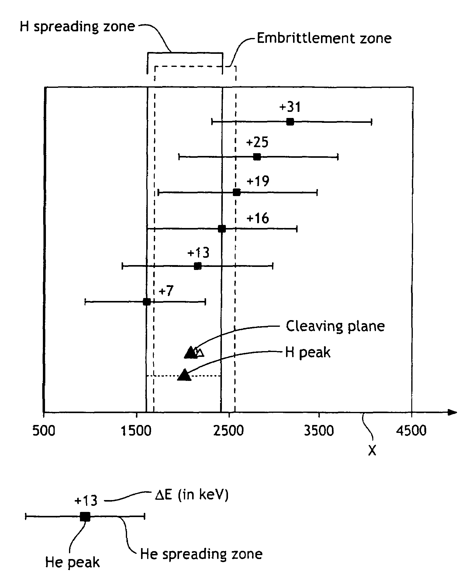
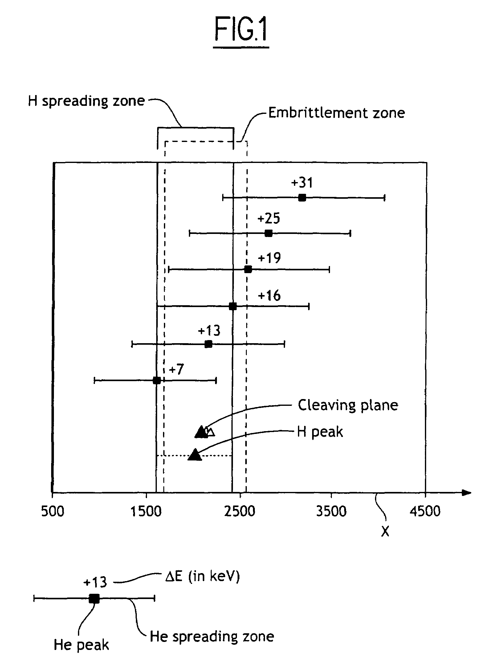
[0030]In order to fill the unresolved needs of the prior art, the invention proposes, according to a first aspect, a method for producing a structure comprising a thin layer of semiconductor material on a substrate, comprising the steps consisting in:[0031]performing a co-implantation of at least two different species under a face of a donor substrate from which the thin layer must be made, so as to create an embrittlement zone in the thickness of the donor substrate,[0032]placing the face of the donor substrate into close contact with a support substrate, after it has undergone implantation,[0033]detaching the donor substrate at the level of the embrittlement zone, so as to transfer a part of the donor substrate onto the support substrate and to form the thin layer on the latter,

at least a first species being implanted acting essentially chemically for forming platelet-like defects in the donor substrate, at least a second species being implanted acting essentially physically as a ...


PUM


Abstract

A method for producing a semiconductor structure by conducting controlled co-implanting of at least first and second different atomic species into a donor substrate to create an embrittlement zone which defines a thin layer of donor material to be transferred. Implantation energies are selected so that the first and second species are respectively distributed in the donor wafer according to a repartition profile that presents a spreading zone in which each species is mainly distributed at a maximum concentration peak. The implantation doses and energies of the first and second species are selected such that the second species is implanted deeper in the embrittlement zone than the first species spreading zone. The donor substrate is detached at the embrittlement zone to transfer the thin layer to the support substrate while minimizing blister formation in and surface roughness of the transferred layer. Preferably, the implantation dose of the first species is between about 40 to 60 percent of all implantation doses. This method is preferably utilized for forming or producing SeOI (Semiconductor On Insulator) structures.

Description

CROSS-REFERENCE TO RELATED APPLICATIONS[0001]This application is a continuation of International Application PCT / IB2004 / 003300 filed Sep. 21, 2004, the entire content of which is expressly incorporated herein by reference thereto.BACKGROUND[0002]The present invention relates to a method for producing a structure that includes a thin layer of semiconductor material on a substrate. The method includes the steps of:[0003]carrying out implantation of species under a face of a donor substrate from which the thin layer must be made, so as to create an embrittlement zone in the thickness of the donor substrate,[0004]placing the face of the donor substrate into close contact with a support substrate, after it has undergone implantation,[0005]detaching the donor substrate at the level of the embrittlement zone, so as to transfer a part of the donor substrate onto the support substrate and to form the thin layer on the latter.[0006]The invention relates more precisely to the above-mentioned i...

Claims


Application Information

Patent Timeline
Patent Type & Authority Patents(United States)
IPC IPC(8): H01L21/30
CPCH01L21/26506H01L21/76254
Inventor BEN MOHAMED, NADIANGUYEN, NGUYET-PHUONGAKATSU, TAKESHIBOUSSAGOL, ALICESUCIU, GABRIELA
Owner SOITEC SA
Why Eureka
Try Eureka