Display device and electronic device

a technology of electronic devices and display devices, applied in the field of display devices, can solve the problems of difficult thinness of the display portion, and achieve the effect of convenient mounting and higher added value of portable information equipmen

Inactive Publication Date: 2008-02-19
SEMICON ENERGY LAB CO LTD
View PDF29 Cites 103 Cited by
  • Summary
  • Abstract
  • Description
  • Claims
  • Application Information

AI Technical Summary

Benefits of technology

[0015]A sub-display screen of conventional portable information equipment is limited to a small size because of the space and the cost. However, according to the invention, a large screen can be mounted in the portable information equipment as a sub-display screen. Further, a function of switching between vertical and horizontal display can be easily mounted, leading to higher added value of the portable information equipment.
[0016]In addition, by utilizing a self-light emitting element which does not require a backlight, a quite thin and light display device can be fabricated.

Problems solved by technology

For example, when the portable information equipment which can display on both screens is fabricated by using a liquid crystal display, a display portion thereof is quite difficult to be thin since a backlight or the like has to be disposed between the two screens.

Method used


Image

  • Display device and electronic device
  • Display device and electronic device
  • Display device and electronic device

Examples


embodiment mode 1

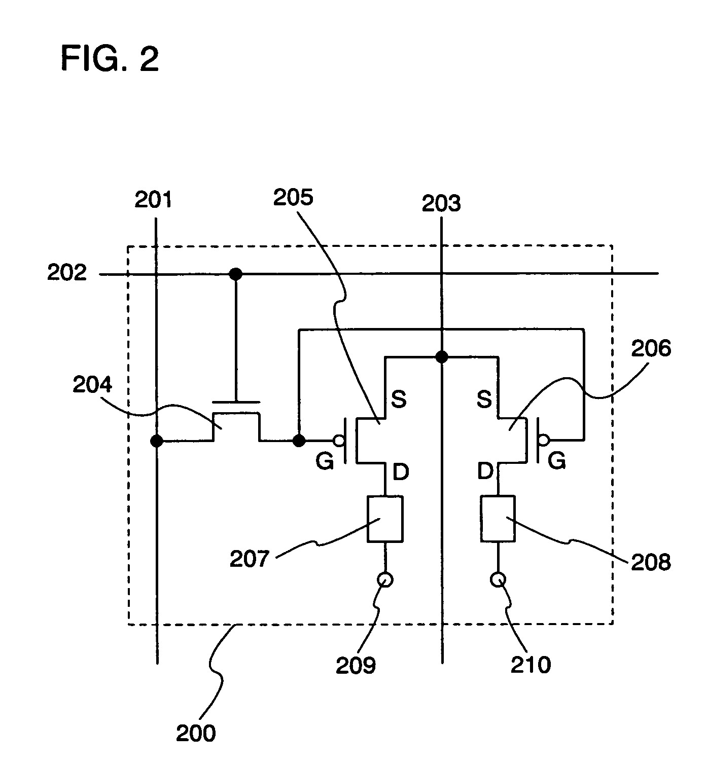
[0028]FIG. 2 shows an embodiment mode of the invention. Note that a thin film transistor (TFT) is used as a switching element and a driving element herein, though the invention is not exclusively limited to this. A MOS transistor, an organic transistor, a molecule transistor or the like may be employed as well. Since it is difficult to differentiate a source region and a drain region of a TFT in accordance with the structure or the operating condition, one of the two regions is referred to as a first electrode and the other thereof is referred to as a second electrode.

[0029]In FIG. 2, a region surrounded by a dotted line frame 200 shows one pixel, which comprises a source signal line 201, a gate signal line 202, a current supply line 203, a switching TFT 204, a first driving TFT 205, a second driving TFT 206, a first light emitting element 207, and a second light emitting element 208. Each pixel includes a first region in which light from the first light emitting element 207 can be ...

embodiment mode 2

[0035]Described mainly in this embodiment mode is a circuit configuration.

[0036]FIG. 5A shows an example of a configuration of the display device according to the invention. A pixel portion 501 is formed on a substrate 500, and a source signal line driver circuit 502, a first gate signal line driver circuit 503, and a second gate signal line driver circuit 504 are formed in the peripheral portion of the pixel portion. A control signal input to each of the driver circuits and a current supply to a current supply line 505 are performed through a flexible printed circuit (FPC) 506. A portion denoted by 510 in FIG. 5A corresponds to one pixel, which is shown in more detail in FIG. 5B.

[0037]In FIG. 5B, a portion surrounded by a dotted line frame 520 is a pixel which comprises a source signal line 521, a first gate signal line 522, a second gate signal line 523, a current supply line 524, a first switching TFT 525, a second switching TFT 526, a first driving TFT 527, a second driving TFT ...

embodiment

Embodiment 1

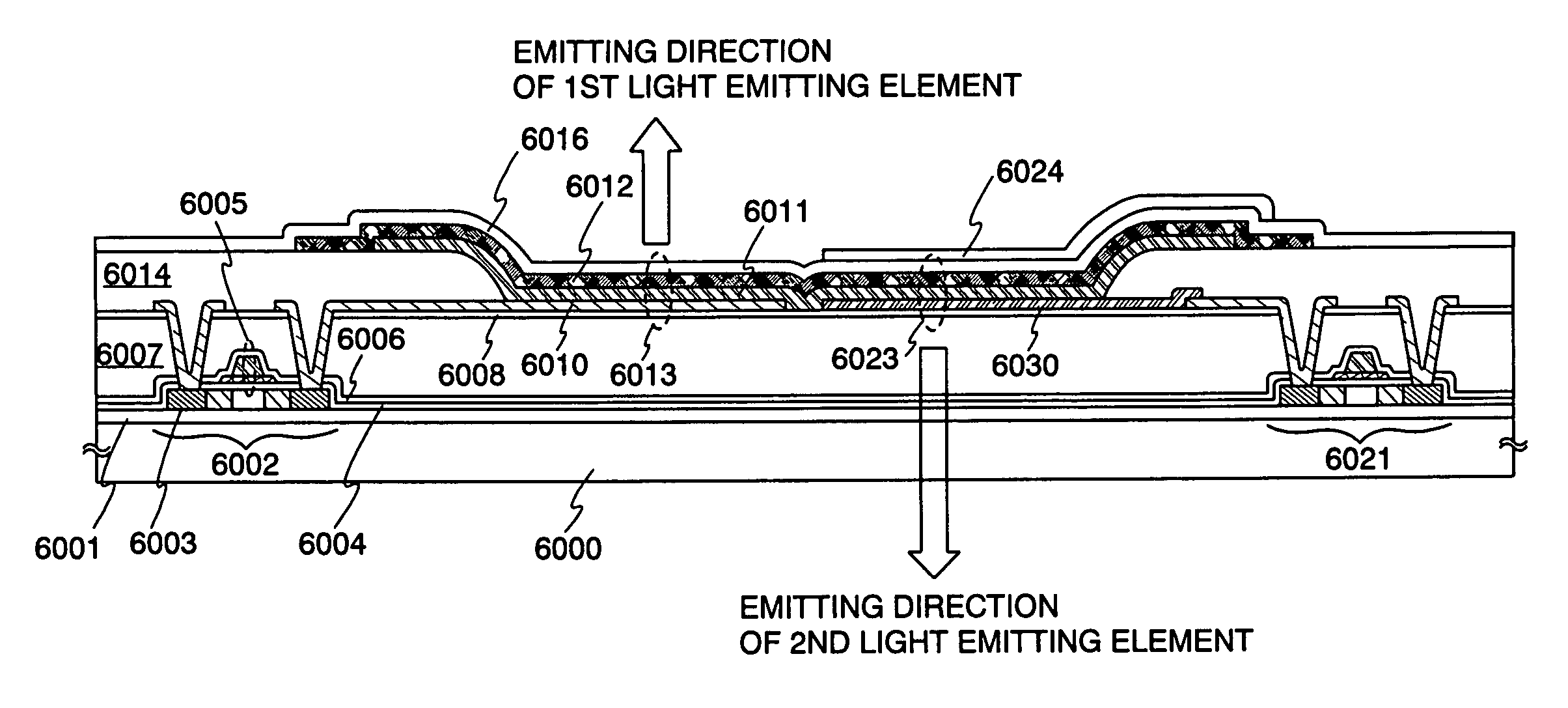
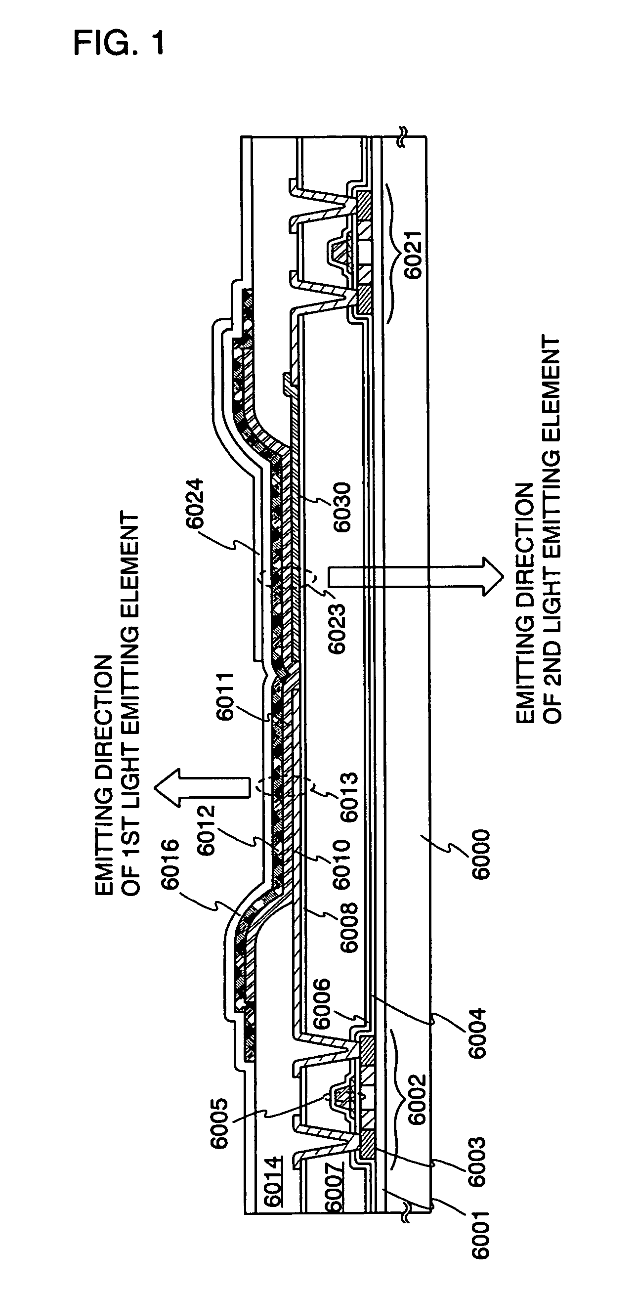
[0045]A pixel configuration of the display device according to the invention is described with reference to FIG. 1.

[0046]In FIG. 1, a base film 6001 is formed on a substrate 6000, and a first driving TFT 6002 and a second driving TFT 6021 are formed on the base film 6001.

[0047]The first driving TFT 6002 comprises an active layer 6003, a gate electrode 6005, and a gate insulating film 6004 which is sandwiched between the active layer 6003 and the gate electrode 6005. It is to be noted that although the gate electrode 6005 is formed of two layers having the upper layer and the lower layer with different widths in FIG. 1, it is not limited to this and may be formed of a single layer or multiple layers.

[0048]In addition, the first driving TFT 6002 is covered with a first interlayer insulating film 6006, and a second interlayer insulating film 6007 and a third interlayer insulating film 6008 are formed in this order over the first interlayer insulating film 6006.

[0049]Note th...


PUM


Abstract

A display device capable of displaying on both screens and switching between vertical and horizontal display, and a driving method thereof. Each pixel comprises a first region including a first light emitting element, and a second region including a second light emitting element. The first region has a bottom emission structure whereas the second region has a top emission structure. The display device comprises a source signal line driver circuit for driving the pixel, a first gate signal line driver circuit having a scan direction perpendicular to that of the source signal line driver circuit, and a second gate signal line driver circuit having a scan direction perpendicular to that of the first gate signal line driver circuit. In a normal display, the first gate signal line driver circuit performs perpendicular scanning, and when switching between vertical and horizontal display, the second gate signal line driver circuit performs perpendicular scanning.

Description

TECHNICAL FIELD[0001]The present invention relates to a display device comprising a light emitting element. More particularly, the invention relates to portable information equipment such as mobile phones and PDAs.BACKGROUND ART[0002]In recent years, a display device using a self-light emitting element typified by an electroluminescence (EL) element and the like has been researched and developed to replace a liquid crystal display (LCD) using a liquid crystal element for a pixel. The display device using a self-light emitting element has the advantages of high image quality, wide viewing angle, and being thin and light because of requiring no backlight. Therefore, it is expected to be widely used as a display panel of a mobile phone or as a display device.[0003]On the other hand, the portable information equipment is required to have high added value as the intended purpose thereof is diversified. Thus, the equipment provided with a sub-display screen on the back side of the main di...

Claims


Application Information

Patent Timeline
Patent Type & Authority Patents(United States)
IPC IPC(8): G09G3/30G09F9/30G09G3/20G09G3/32G09G5/00H01L27/32H05B33/14H05B33/26H05B44/00
CPCG09G3/32H01L27/3267G09G2300/0443G09G2300/0809H01L2251/5323G09G2340/0492G09G2300/0842H10K59/128H10K2102/3031
Inventor KOYAMA, JUNYAMAZAKI, YUTANADA, YOSHIFUMISEO, SATOSHINISHI, TAKESHINAKAMURA, YASUOYAMAZAKI, SHUNPEI
Owner SEMICON ENERGY LAB CO LTD
Why Eureka
Try Eureka