Fast evaluation of average critical area for IC layouts

a critical area and layout technology, applied in the direction of cad circuit design, program control, instruments, etc., can solve the problems of random defect yield loss, calculation of geographic union can be extremely time-consuming, and only at the expense of accuracy

Active Publication Date: 2008-03-18
SYNOPSYS INC
View PDF2 Cites 23 Cited by
  • Summary
  • Abstract
  • Description
  • Claims
  • Application Information

AI Technical Summary

Problems solved by technology

As VL SI technology moves to deep sub micron, manufacturability and yield related issues become increasingly important.
One important factor is random defect yield loss, which is related to the yield loss caused by contamination particles.
One problem with the conventional shape expansion methods is that calculation of a geographic union can be extremely time consuming.
Some methods approximate the geographic union, but only at the expense of accuracy.
Other methods do not even attempt to approximate the geographic union, and simply add all the critical area contributions together.
Many conventional shape expansion methods also suffer because they require a separate critical area calculation for each defect size of interest.
Because each critical area calculation is so expensive, the number of discrete defect sizes for which it is calculated is often reduced, thereby degrading accuracy of the results.
If accuracy is to be improved by increasing the number of discrete defect sizes at which the critical area calculation is made, then runtimes can easily become prohibitive.
Another problem with conventional shape expansion methods is that there is no explicit formula available for total critical area.
Thus it cannot be used to evaluate critical area as part of cost function for layout optimization.
But accurate estimation may still require huge runtimes due to the need to test huge numbers of randomly generated defects.

Method used


Image

  • Fast evaluation of average critical area for IC layouts
  • Fast evaluation of average critical area for IC layouts
  • Fast evaluation of average critical area for IC layouts

Examples


Embodiment Construction

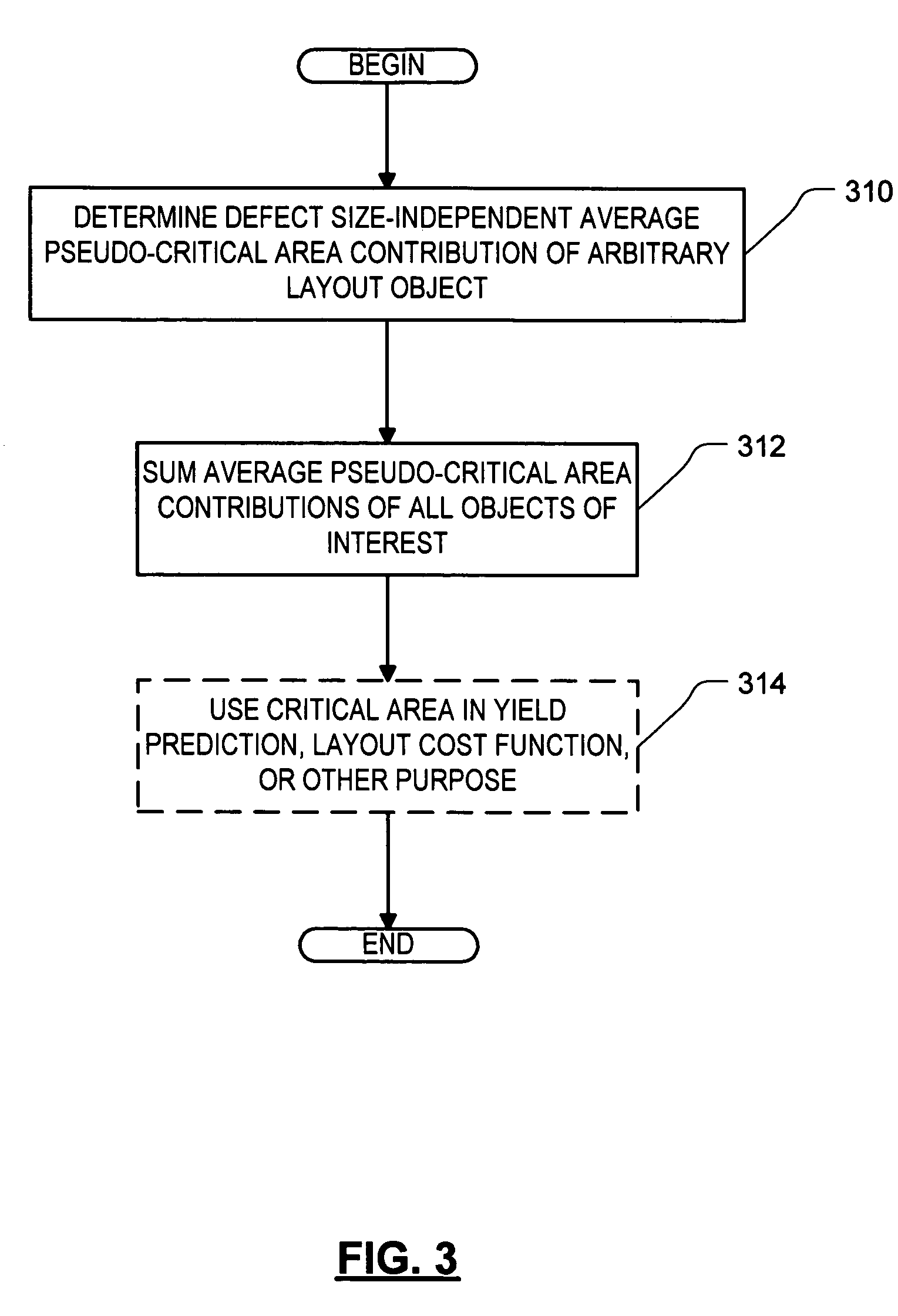
[0015]The following description is presented to enable any person skilled in the art to make and use the invention, and is provided in the context of a particular application and its requirements. Various modifications to the disclosed embodiments will be readily apparent to those skilled in the art, and the general principles defined herein may be applied to other embodiments and applications without departing from the spirit and scope of the present invention. Thus, the present invention is not intended to be limited to the embodiments shown, but is to be accorded the widest scope consistent with the principles and features disclosed herein.

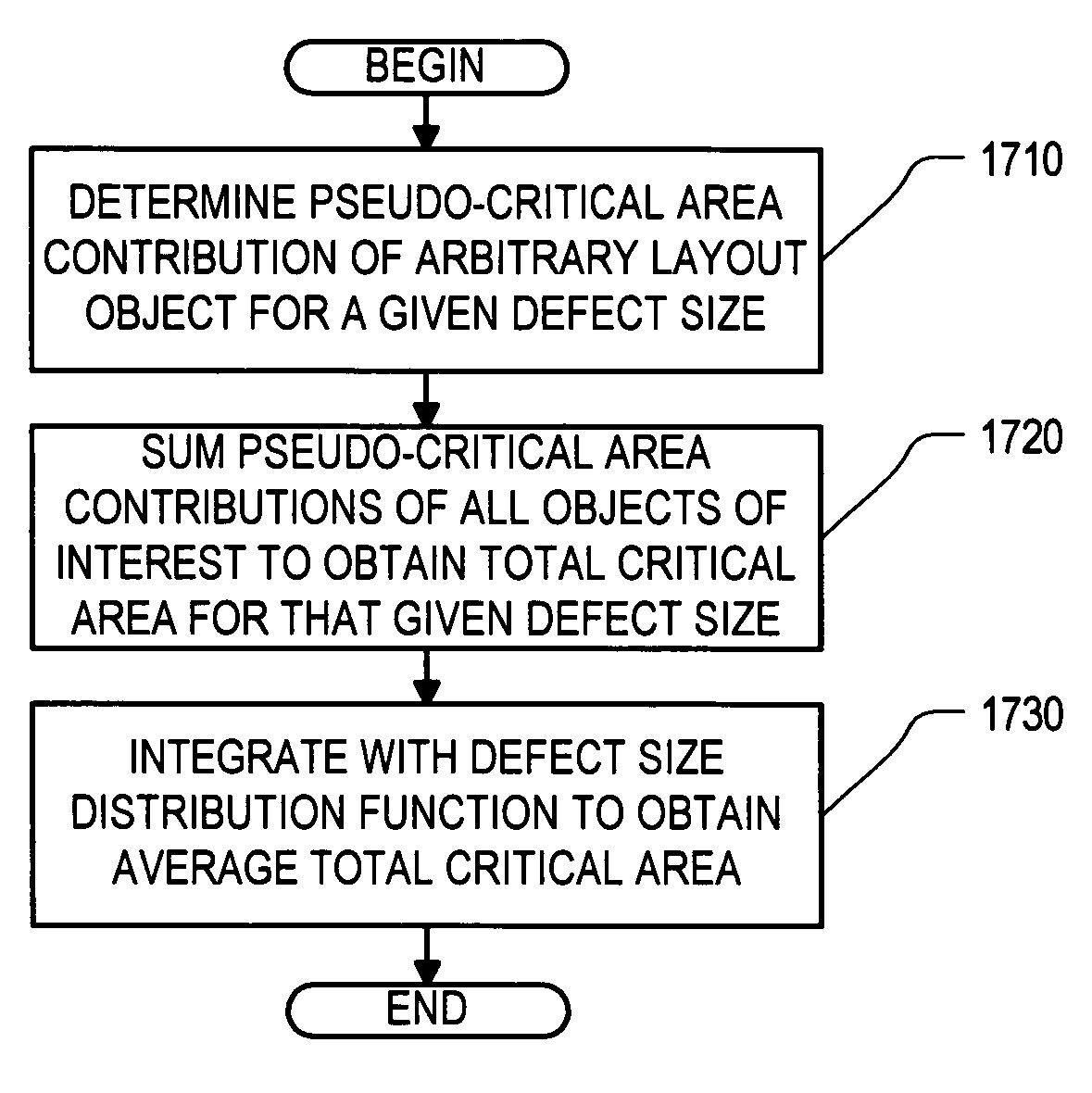
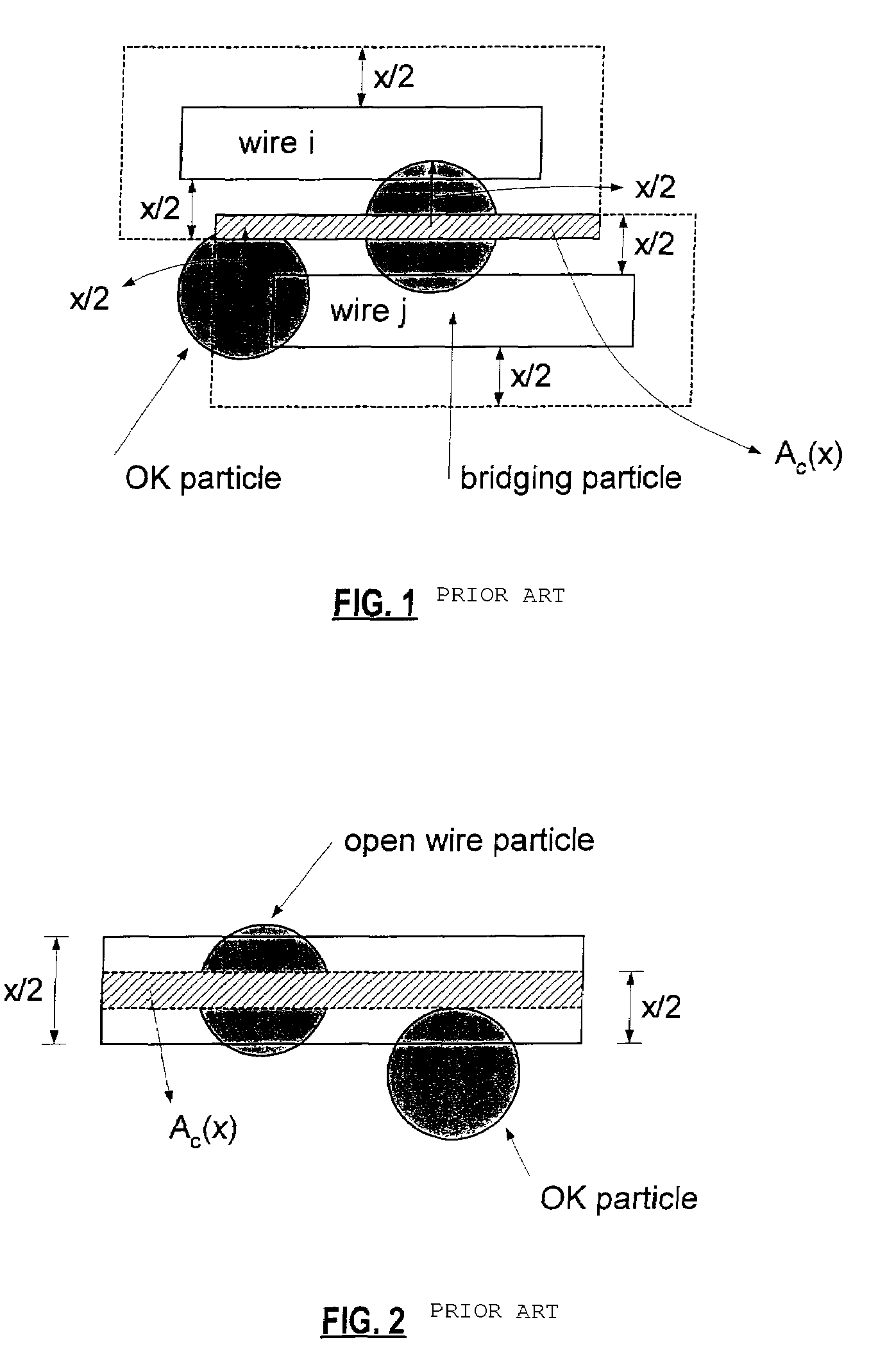
[0016]The critical area Ac is defined as the total area of the regions on the layout where the contamination particles must fall to cause functional failures (such as open and short circuit failures). For purposes of the present discussion, contamination particles are approximated as discs, and the location of the centerpoint is considered to b...


PUM


Abstract

Method and apparatus for approximating the average critical area of a layout or layout region, involving summing, over all the object segments of interest, respective critical area contribution values that are dependent upon particular layout parameters of the objects, each of the contribution values being representative of a plurality of defect sizes, and being defined such that for each defect size in the plurality of defect sizes, and for a particular defect type, the contribution values collectively count all critical areas arising due to the object segments of interest only once.

Description

BACKGROUND[0001]1. Field of the Invention[0002]The invention relates to integrated circuit fabrication, and more particularly to methods for determining the average critical area of a particular layout.[0003]2. Description of Related Art[0004]As VL SI technology moves to deep sub micron, manufacturability and yield related issues become increasingly important. Yield loss can be caused by many factors. One important factor is random defect yield loss, which is related to the yield loss caused by contamination particles. The design related parameter required for modeling random defect yield is sometimes called the critical area.[0005]Critical Area measures a design's sensitivity to the random particle defects. Much work has been done on extracting and calculating the critical area for a given design layout. The main approaches fall into the two main categories: Shape Expansion based methods and Monte Carlo methods. Conventional shape expansion based methods generally attempt to calcul...

Claims


Application Information

Patent Timeline
Patent Type & Authority Patents(United States)
IPC IPC(8): G06F17/50
CPCG06F17/5068G06F30/39
Inventor SU, QINGSINHA, SUBARNAREKHACHIANG, CHARLES C.
Owner SYNOPSYS INC
Why Eureka
Try Eureka