

Surface defect data display and management system and a method of displaying and managing a surface defect data
a technology of defect data and management system, which is applied in the direction of mechanical control devices, instruments, semiconductor/solid-state device testing/measurement, etc., can solve the problems of giving a fatal fault to the operation of an integrated circuit, the difficulty of selecting the surface the large problem of how to observe the defect visually by the operator, etc., to achieve easy selection and high risk score
- Summary
- Abstract
- Description
- Claims
- Application Information
AI Technical Summary
Benefits of technology
Problems solved by technology
Method used
Image

Examples
Embodiment Construction
[0027]Embodiments of the invention will now be described in greater detail by making reference to the accompanying drawings as necessary.
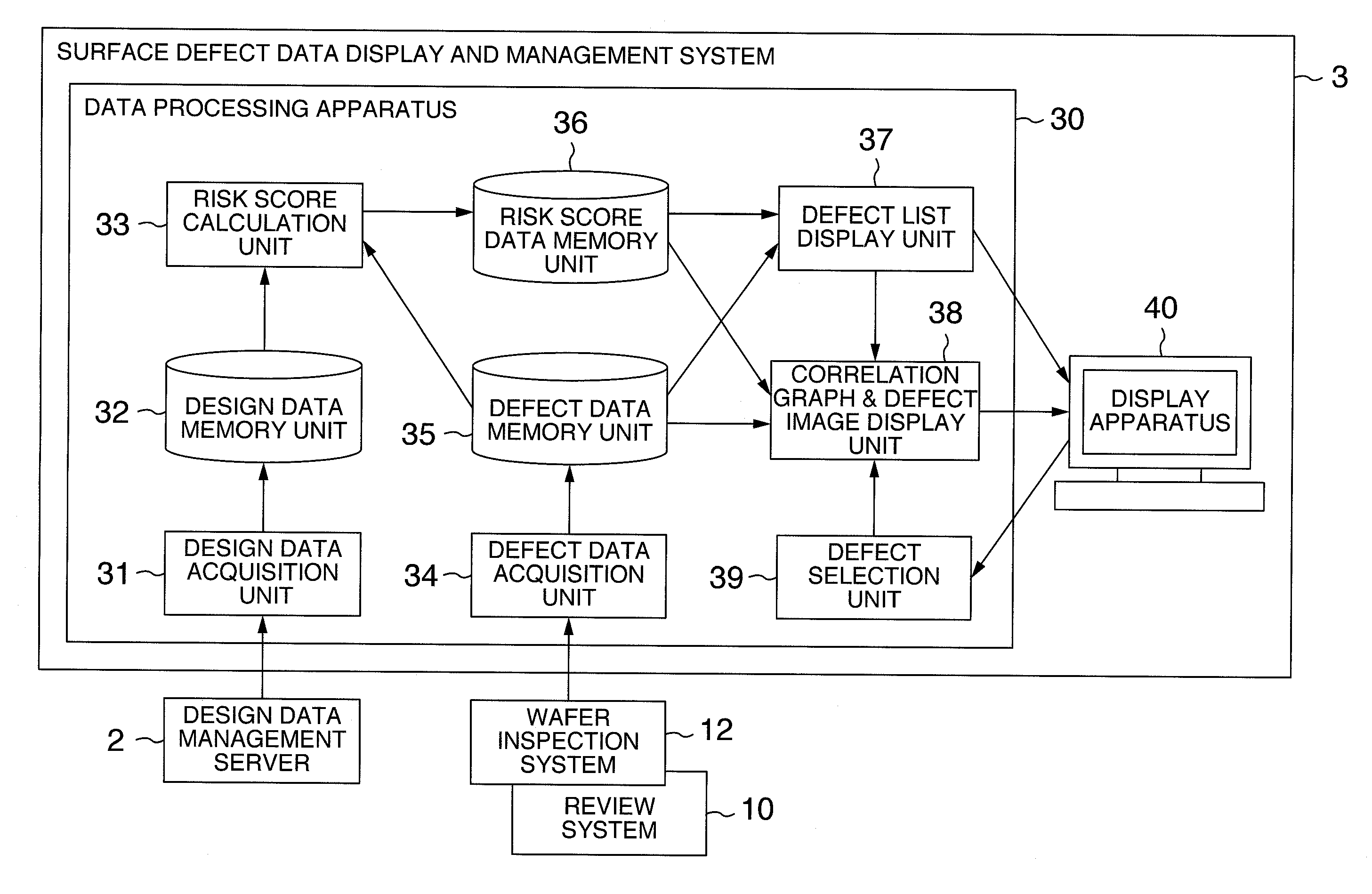
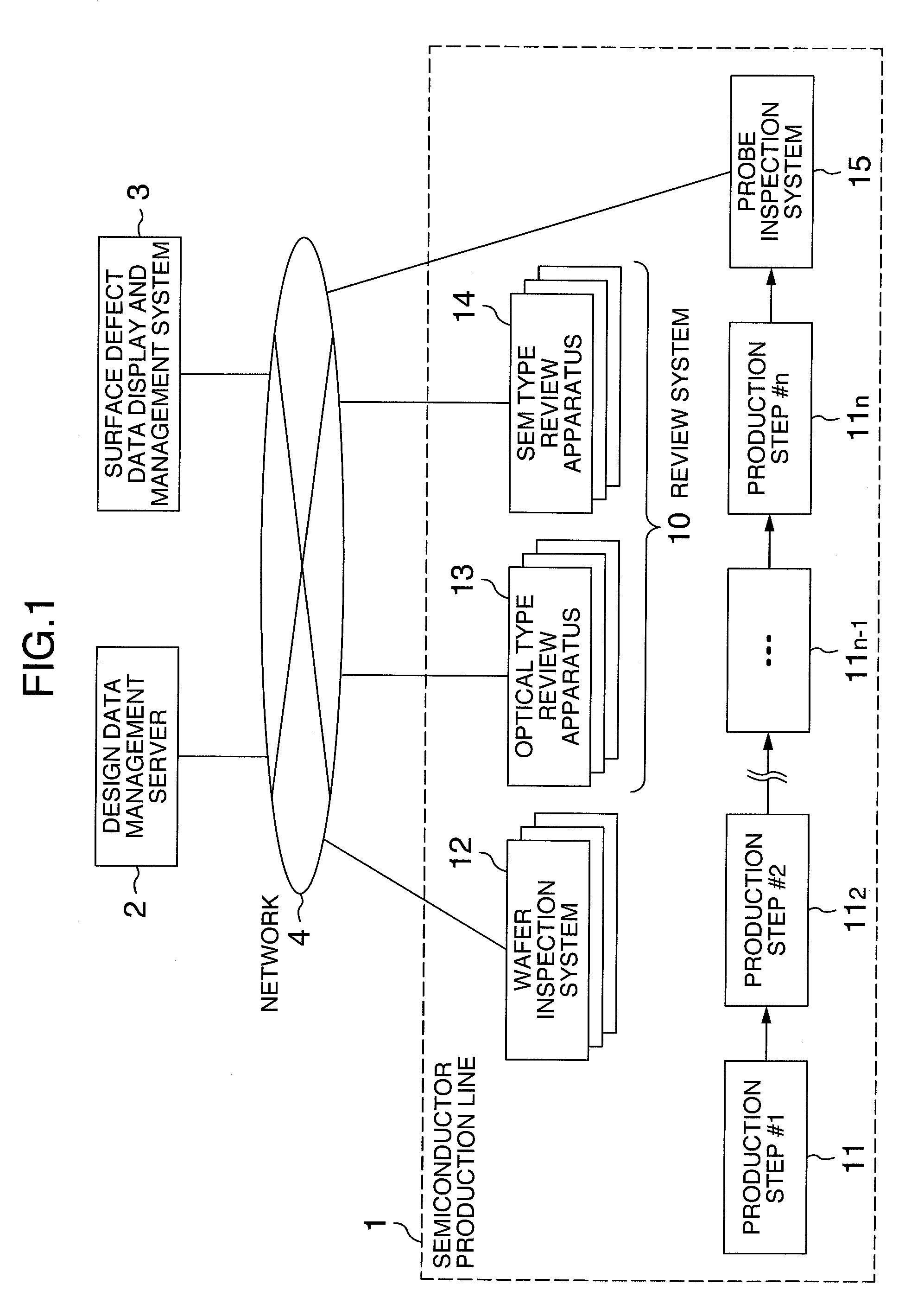
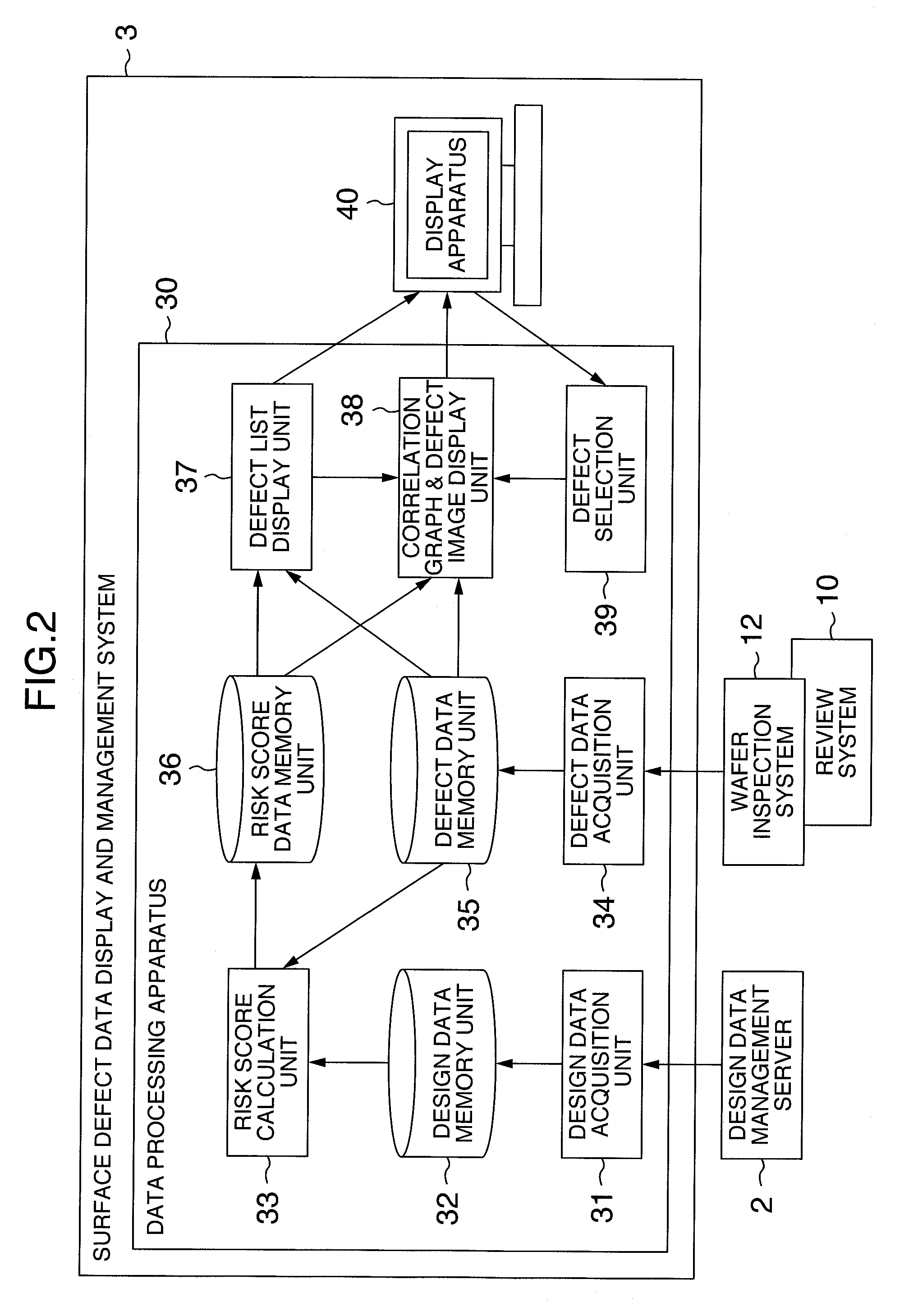
[0028]Referring first to FIG. 1, there is illustrated an example of construction of an overall system to which a surface defect data display and management system according to an embodiment of the invention is applied.
[0029]As shown in FIG. 1, a semiconductor production line 1 is comprised of a plurality of production steps 11 executable in a so-called clean room and through the plural production steps 11, circuit patterns of devices and wiring are formed sequentially on, for example, a silicon wafer to manufacture an integrated circuit on the wafer. At that time, in a final one of the production steps 11, a probe inspection system 15 is provided, so that the integrated circuit formed on the wafer is inspected electrically to obtain quality information such as production yield.
[0030]In correspondence with the individual production steps 11, a wafer...
PUM
 Abstract
Description
Claims
Application Information