

Plasma processing of tungsten using a gas mixture comprising a fluorinated gas and oxygen
a technology of fluorinated gas and oxygen, which is applied in the direction of chemistry apparatus and processes, instruments, fluid pressure measurement, etc., can solve the problems of increased substrate rejection, defective circuit structure, and complex integrated circuits that have evolved into complex devices. , to achieve the effect of good selectivity
- Summary
- Abstract
- Description
- Claims
- Application Information
AI Technical Summary
Benefits of technology
Problems solved by technology
Method used
Image

Examples
Embodiment Construction
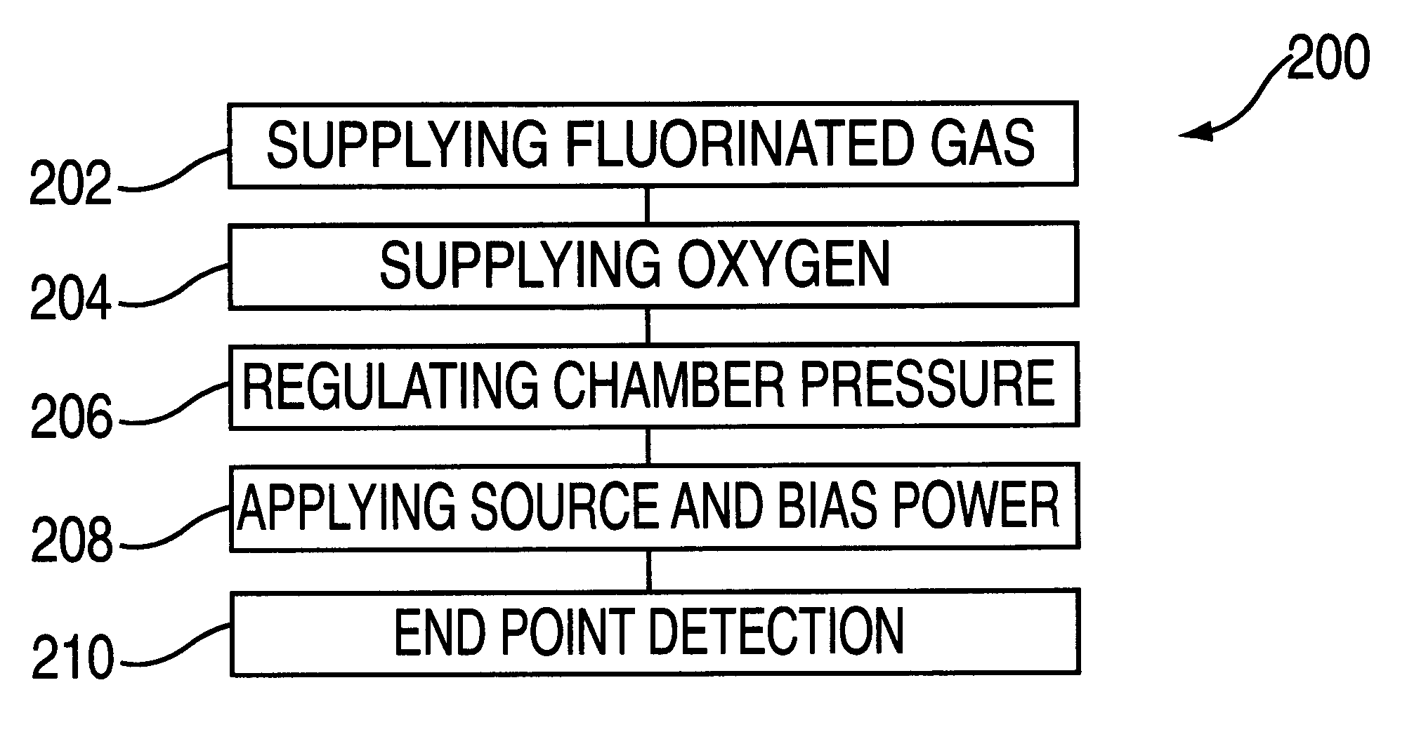
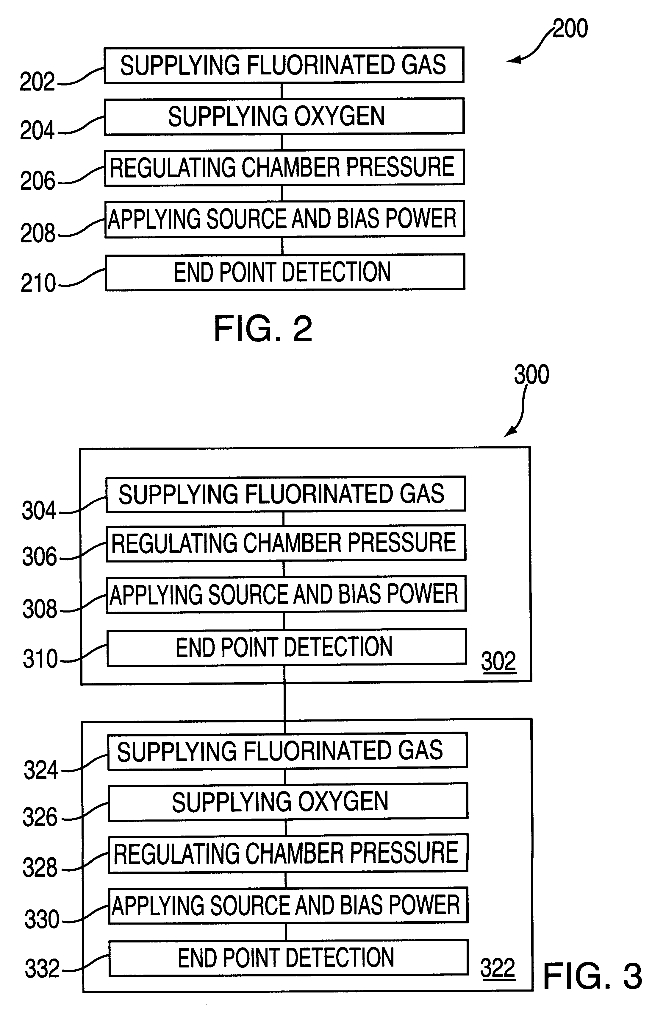
An embodiment of the present invention is a method of etching a substrate comprising a tungsten layer overlying polysilicon. The embodiment of the present invention etches the tungsten to expose the polysilicon material while minimizing the amount of polysilicon removed, i.e., the etch process exhibits good selectivity between tungsten and polysilicon. The etch process of the present invention can be reduced to practice in a number of etching systems capable of plasma processing tungsten. One such system is a Decoupled Plasma Source (DPS) Centura etch system available from Applied Materials, Inc., of Santa Clara, Calif.
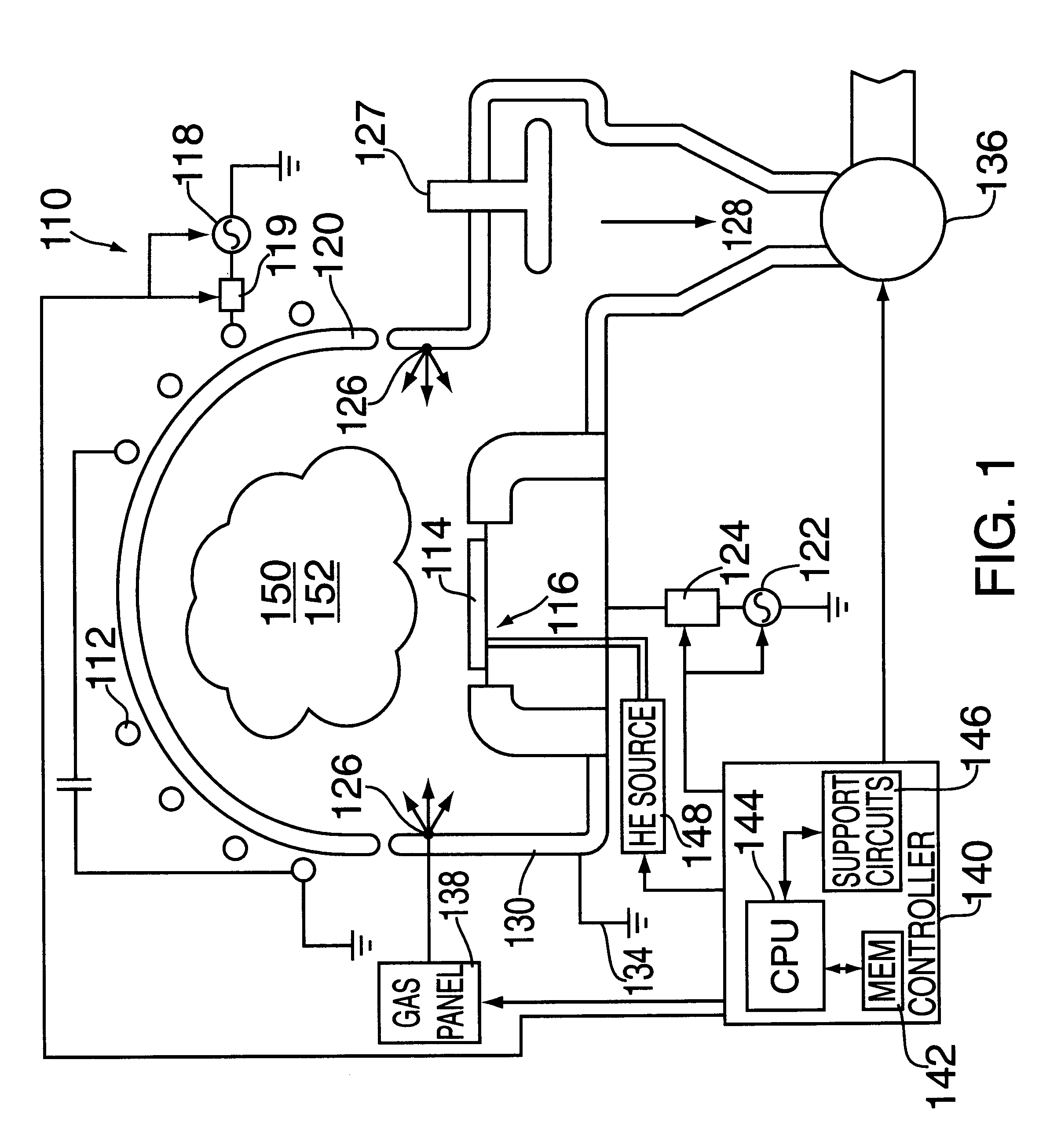
FIG. 1 depicts a schematic diagram of the DPS etch process chamber 110, that comprises at least one inductive coil antenna segment 112, positioned exterior to a dielectric, dome-shaped ceiling 120 (referred hereinafter as the dome 120). The antenna segment 112 is coupled to a radio-frequency (RF) source 118 that is generally capable of producing an RF signal having a ...
PUM
| Property | Measurement | Unit |
|---|---|---|
| power | aaaaa | aaaaa |
| bias power | aaaaa | aaaaa |
| pressure | aaaaa | aaaaa |
Abstract
Description
Claims
Application Information