Switching power supply device
a technology of switching power supply and power supply circuit, which is applied in the direction of electric variable regulation, process and machine control, instruments, etc., can solve the problems of unstable operation of the control circuit on-time control of the high-side switching device, and further reduction of power consumption. , to achieve the effect of reducing power consumption and device size, increasing efficiency
- Summary
- Abstract
- Description
- Claims
- Application Information
AI Technical Summary
Benefits of technology
Problems solved by technology
Method used
Image
Examples
embodiment 1
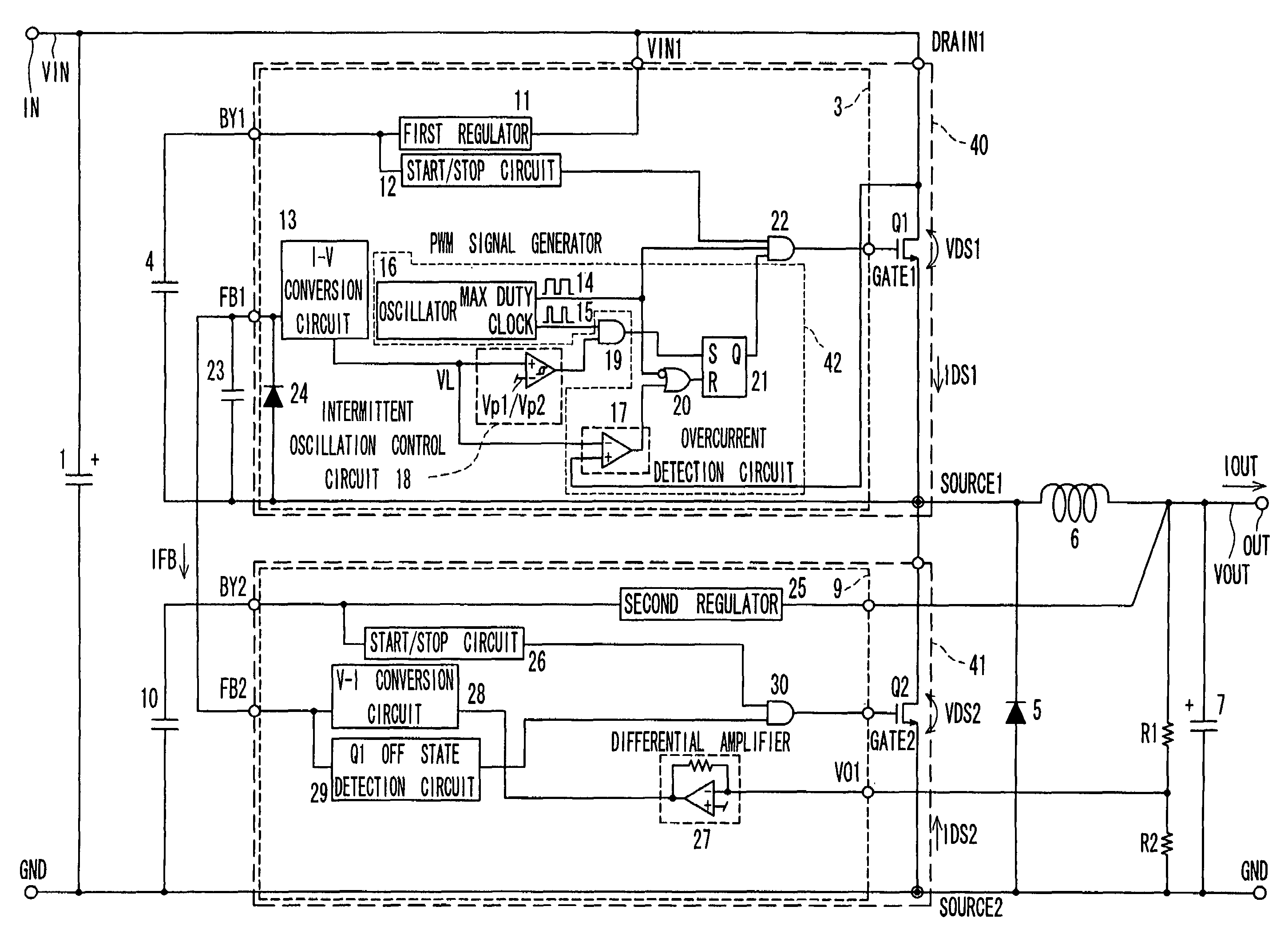
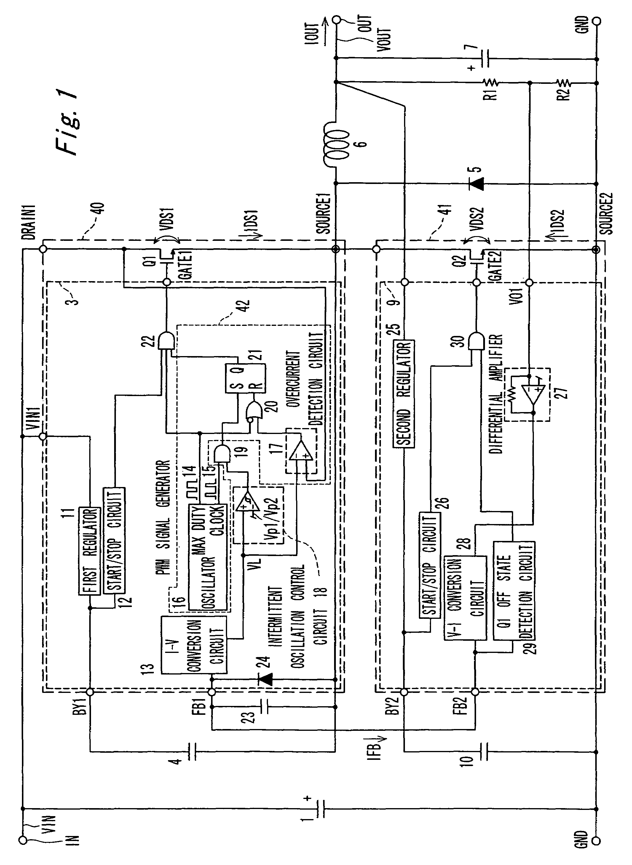
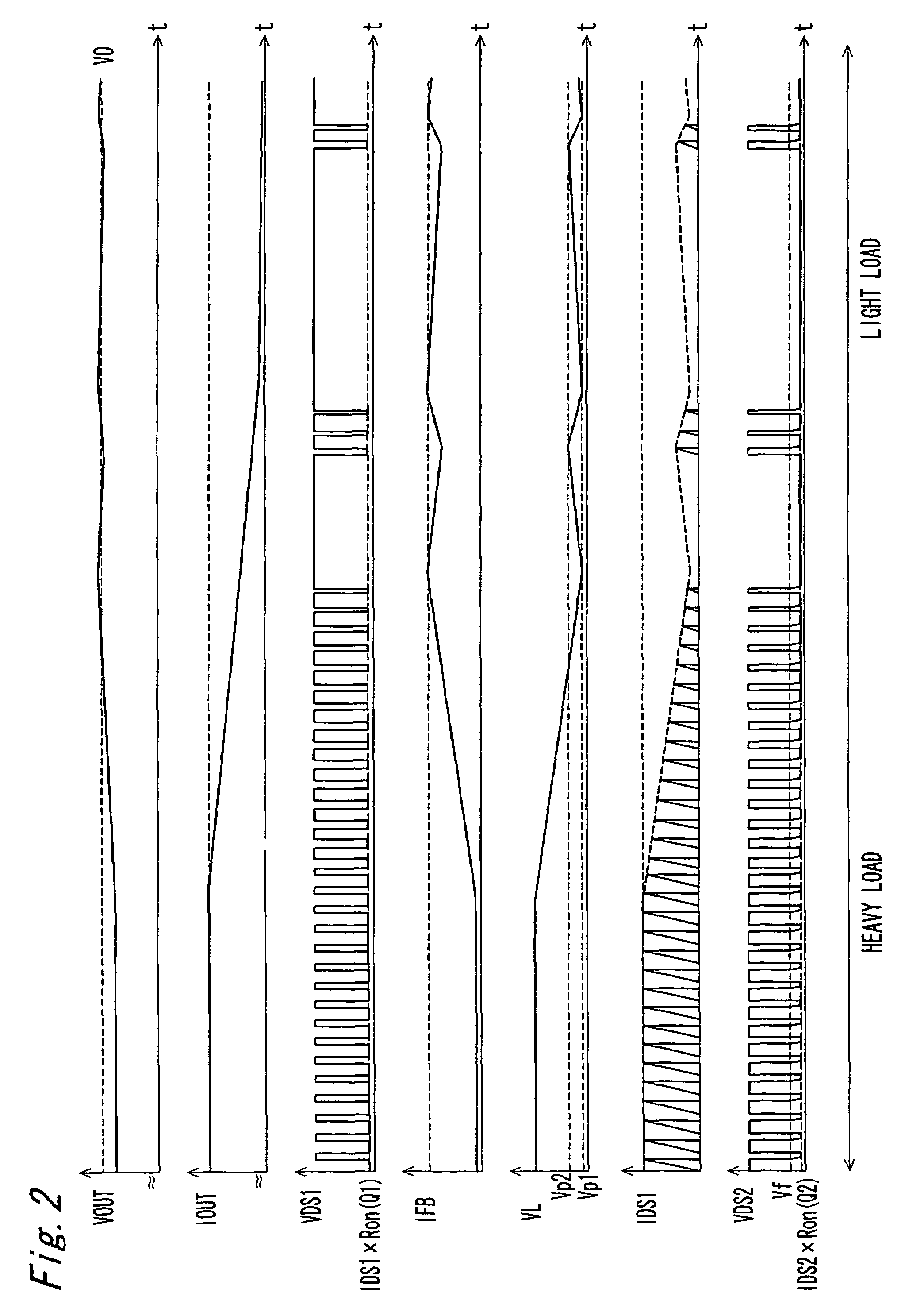
[0053]FIG. 1 shows a switching power supply device according to a first embodiment of the invention, and FIG. 2 shows the operating waves when the output load of the switching power supply in this first embodiment of the invention changes from a heavy load to a light load. In FIG. 1 and FIG. 2 the first supply voltage VIN is the voltage input to the input terminal IN from the first power supply voltage supply device where the ground potential of the ground terminal GND is the lowest potential; the second supply voltage VOUT is the voltage output from output terminal OUT where the lowest potential is the ground potential; IOUT is the current level at output terminal OUT; VDS1 is the DRAIN1 voltage of switching device Q1; IFB is the FB1 node current (=FB2 node current); IDS1 is the DRAIN1 current flowing through switching device Q1.
[0054]The switching power supply device according to this first embodiment of the invention comprises input capacitor 1, switching device Q1 and switching ...
second embodiment
[0075]FIG. 3 shows a switching power supply device according to a second embodiment of the invention. This embodiment of the invention renders a negative output power supply by connecting the negative terminal of the input capacitor 1 connected to the anode of the third diode 5 in FIG. 1 to the positive terminal of the output capacitor 7. As a result, the minimum potential of the second supply voltage VOUT is equal to the minimum potential of the first supply voltage VIN minus second supply voltage VOUT.
[0076]More specifically, the polarity of the second supply voltage is the same as the polarity of the first supply voltage in the first embodiment of the invention shown in FIG. 1, but in the second embodiment of the invention shown in FIG. 3 the polarity of the second supply voltage is the opposite of the polarity of the first supply voltage. The power supply operation is the same as in the switching power supply device of the first embodiment of the invention.
[0077]In addition to t...
third embodiment
[0078]FIG. 4 shows a switching power supply device according to a third embodiment of the invention. In this embodiment of the invention power is supplied to the second regulator 25 of the control circuit 9 not from second supply voltage VOUT but instead directly from first supply voltage VIN. The power supply operation is the same as in the switching power supply device of the first embodiment of the invention.
[0079]In addition to the effects afforded by the first embodiment of the invention, using a switching power supply device according to this third embodiment of the invention enables easily lowering the output voltage.
PUM
| Property | Measurement | Unit |
|---|---|---|
| input supply voltage | aaaaa | aaaaa |
| voltage | aaaaa | aaaaa |
| source voltage | aaaaa | aaaaa |
Abstract
Description
Claims
Application Information


