Semiconductor package, manufacturing method thereof and IC chip

a technology of semiconductor devices and stack packages, applied in the direction of semiconductor devices, semiconductor/solid-state device details, electrical apparatus, etc., can solve the problems of reducing reliability, complicated stack structure, and involving difficult and/or inefficient stacking processes

Active Publication Date: 2008-04-08
SAMSUNG ELECTRONICS CO LTD
View PDF16 Cites 78 Cited by
  • Summary
  • Abstract
  • Description
  • Claims
  • Application Information

AI Technical Summary

Problems solved by technology

Although the conventional methods are generally thought to be acceptable, they are not without shortcomings.
For example conventional techniques may result in complicated stack structures and / or conventional techniques may involve difficult and / or inefficient stacking processes.
Further, connection terminals connecting upper and lower bare chips may be exposed to the external environment, and this may reduce reliability.
The connection terminals (which may be arranged on the outside of bare chips) may lead to increased package size.

Method used


Image

  • Semiconductor package, manufacturing method thereof and IC chip
  • Semiconductor package, manufacturing method thereof and IC chip
  • Semiconductor package, manufacturing method thereof and IC chip

Examples


Embodiment Construction

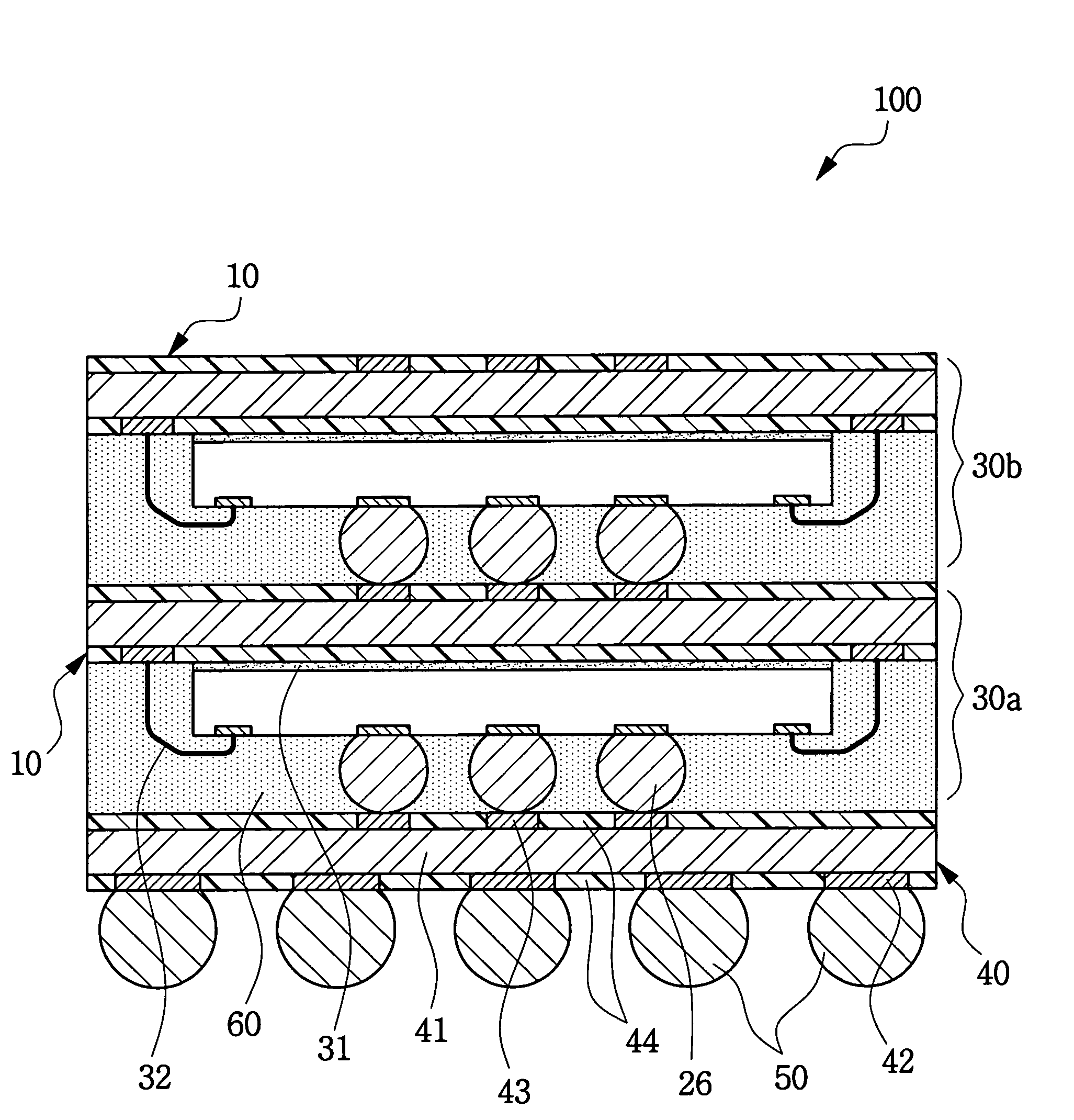
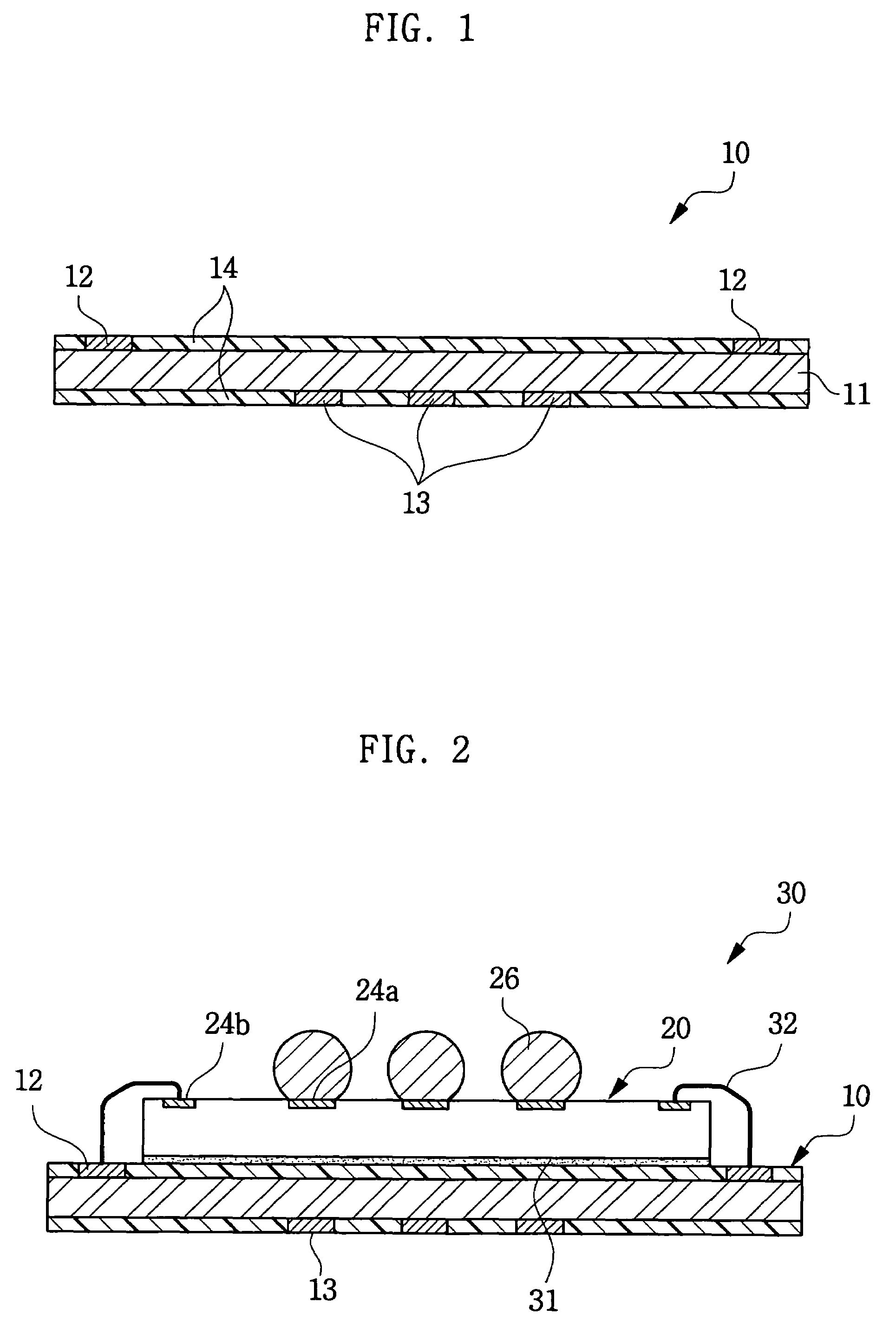
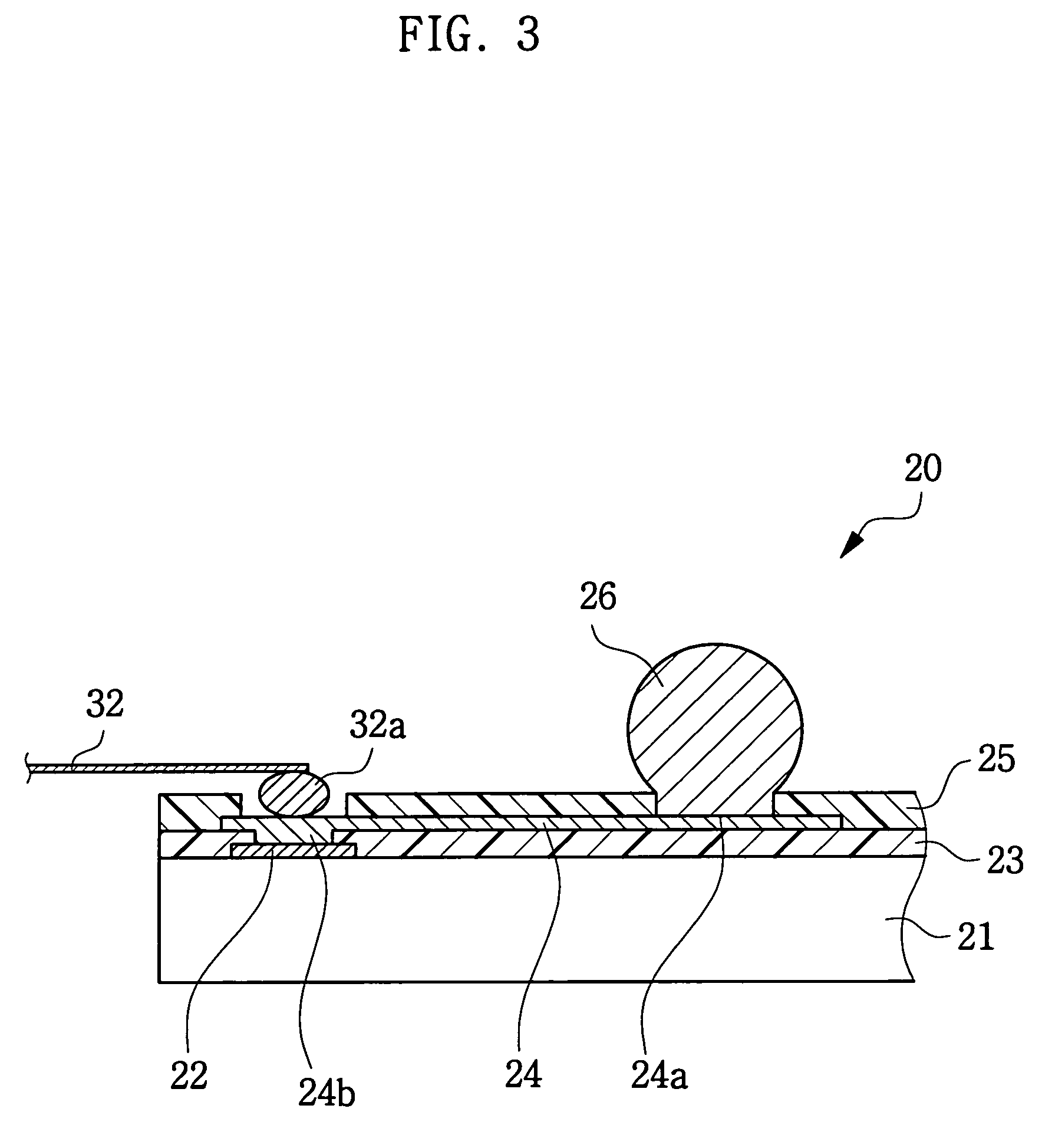
[0024]Example, non-limiting embodiments of the present invention will now be described more fully with reference to the accompanying drawings. This invention may, however, be embodied in many different forms and should not be construed as limited to the example embodiments set forth herein. Rather, the disclosed embodiments are provided so that this disclosure will be thorough and complete, and will fully convey the scope of the invention to those skilled in the art. The principles and features of this invention may be employed in varied and numerous embodiments without departing from the scope of the invention.

[0025]Well-known structures and processes are not described or illustrated in detail to avoid obscuring the present invention.

[0026]An element is considered as being mounted (or provided) “on” another element when mounted (or provided) either directly on the referenced element or mounted (or provided) on other elements overlaying the referenced element. Throughout this disclo...


PUM


Abstract

A package may include a lower unit package and an upper unit package. Each of the unit packages may include a circuit substrate having a lower surface and an upper surface. Wire bonding pads may be provided of the lower surface of the circuit substrate, and chip bonding pads may be provided on the upper surface of the circuit substrate. An IC chip may be provided on the lower surface of the circuit substrate. The IC chip may have an active surface with wire lands and bump lands. Chip bumps may be provided on the bump land. The wire bonding pads of the circuit substrate may be connected to the wire lands of the IC chip using bonding wires. The chip bumps of the upper unit package may be connected to the chip bonding pads of the lower unit package. An IC chip may include a substrate. A conductive layer may be provided on the substrate. The conductive layer may define a bump land for supporting a chip bump and a wire land for connecting to a bonding wire. The bump land and the wire land may be spaced apart from each other on an active surface of the IC chip.

Description

PRIORITY STATEMENT[0001]This U.S. Non-provisional application claims benefit of priority under 35 U.S.C. § 119 from Korean Patent Application No. 2004-104247, filed on Dec. 10, 2004, the entire contents of which are incorporated herein by reference.BACKGROUND[0002]1. Field of the Invention[0003]The present invention relates in general to a semiconductor packaging technique and, more particularly, to a semiconductor chip stack package and a method for manufacturing the semiconductor chip stack package.[0004]2. Description of the Related Art[0005]In an effort to improve integration in a package assembly process, stacking techniques may be employed in which a plurality of integrated circuit (“IC”) chips and / or unit packages may be stacked on a circuit substrate. An example stacking technique may implement bare chip packages.[0006]Bare chip packages (e.g., flip chip packages and wafer level packages) may have IC chips on which conductive bumps may be provided as external connection stru...

Claims


Application Information

Patent Timeline
Patent Type & Authority Patents(United States)
IPC IPC(8): H01L23/02
CPCH01L21/561H01L23/3128H01L24/48H01L24/73H01L24/91H01L24/97H01L25/0657H01L24/05H01L2224/45124H01L2224/45139H01L2224/45144H01L2224/45147H01L2224/48095H01L2224/48145H01L2224/48227H01L2224/48471H01L2224/48475H01L2224/48599H01L2224/48699H01L2224/73207H01L2224/73265H01L2224/85051H01L2224/97H01L2225/06506H01L2225/06517H01L2225/06572H01L2225/06586H01L2924/01004H01L2924/01013H01L2924/01014H01L2924/01028H01L2924/01029H01L2924/01047H01L2924/01079H01L2924/01082H01L2924/014H01L2924/14H01L2924/15311H01L2224/32225H01L2924/01006H01L2924/01033H01L2924/01087H01L24/16H01L2224/0401H01L2224/04042H01L2224/04073H01L2224/05548H01L2224/48799H01L2924/07802H01L2924/00014H01L2224/85H01L2224/83H01L2924/00H01L2924/00012H01L24/45H01L2224/85444H01L2224/85455H01L2924/181H01L2224/05599H01L2224/45015H01L2924/207H01L23/28H01L21/60
Inventor LIM, GWANG-MAN
Owner SAMSUNG ELECTRONICS CO LTD
Why Eureka
Try Eureka