Pixel circuit, display device, and method of driving pixel circuit

a pixel circuit and display device technology, applied in the direction of static indicating devices, identification means, instruments, etc., can solve the problems of difficult realization of large sized and high definition displays, and achieve the effects of good uniformity, reduced luminance deterioration, and reduced mobility

Inactive Publication Date: 2008-04-08
SONY CORP
View PDF12 Cites 14 Cited by
  • Summary
  • Abstract
  • Description
  • Claims
  • Application Information

AI Technical Summary

Benefits of technology

[0072]According to the present invention, even when the I-V characteristic of the EL light emitting element changes by aging, a source-follower output without luminance deterioration can be achieved.
[0073]A source-follower circuit of an n-channel transistor becomes possible, and an n-channel transistor can be used as a drive element of an EL light emitting element by using current anode / cathode electrodes as they are.
[0074]Further, not only the variation of threshold values of drive transistors, but also the variation of mobilities can be greatly suppressed, and image quality having good uniformity can be obtained.
[0075]Further, variation of the threshold values of drive transistors is cancelled out by the reference current, therefore it is not necessary to cancel the threshold value by setting the ON / OFF timing of the switch for each panel, therefore an increase of the number of steps for setting the timing can be suppressed.
[0076]Further, the capacitance inside the pixel can be easily designed, and the capacitance can be made smaller, therefore the pixel area can be reduced, and it becomes possible to make the definition of the panel higher.
[0077]Further, almost all of the voltage change can be coupled with the gate of the drive transistor when inputting the input voltage, therefore variation of the current value for each pixel can be reduced, and a uniform image quality can be obtained.

Problems solved by technology

The former is simple in structure, but has the problems that realization of a large sized and high definition display is difficult and so on.

Method used


Image

  • Pixel circuit, display device, and method of driving pixel circuit
  • Pixel circuit, display device, and method of driving pixel circuit
  • Pixel circuit, display device, and method of driving pixel circuit

Examples


first embodiment

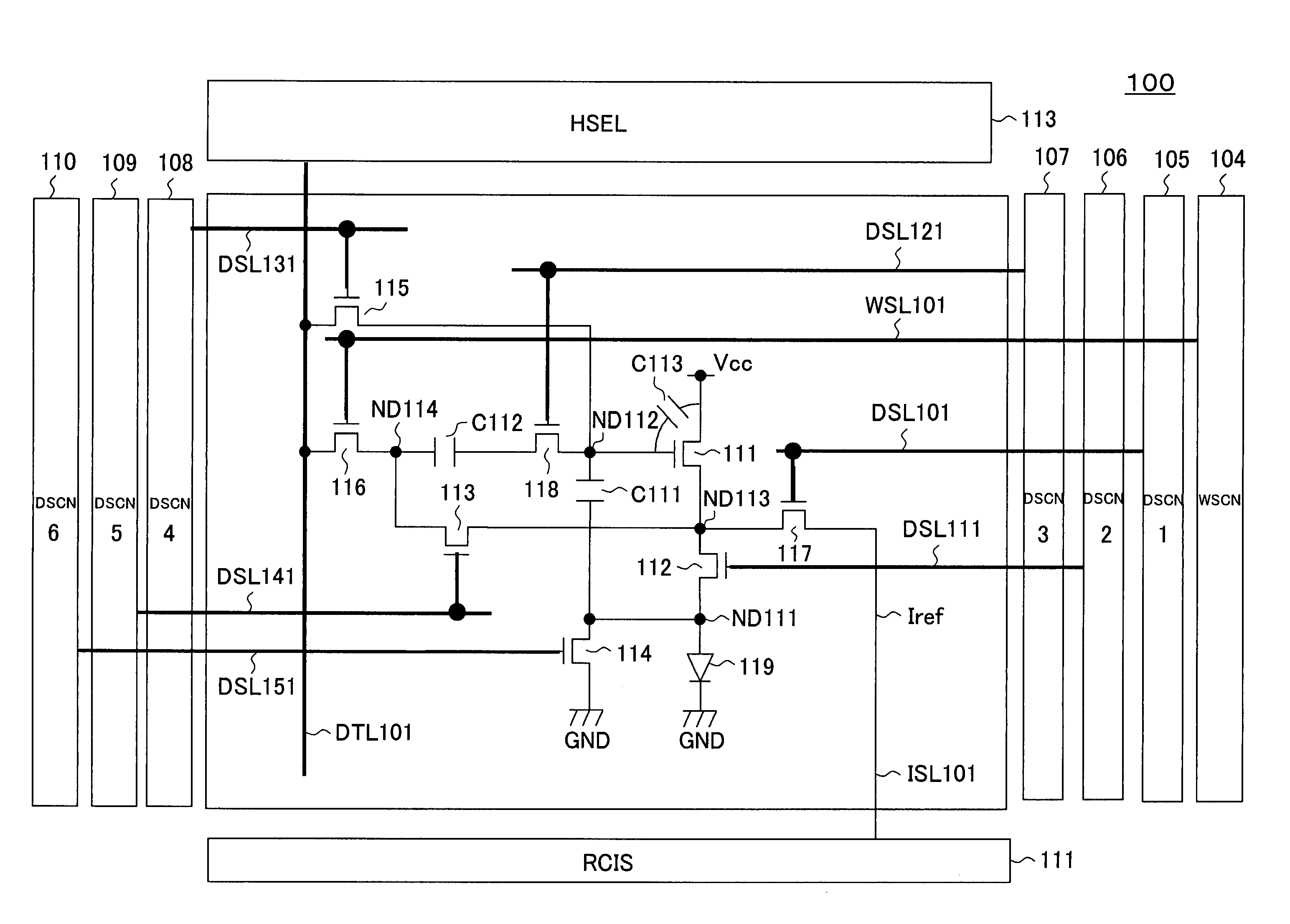
[0129]FIG. 8 is a block diagram showing the configuration of an organic EL display device employing a pixel circuit according to the first embodiment.

[0130]FIG. 9 is a circuit diagram showing a specific configuration of a pixel circuit according to the first embodiment in the organic EL display device of FIG. 8.

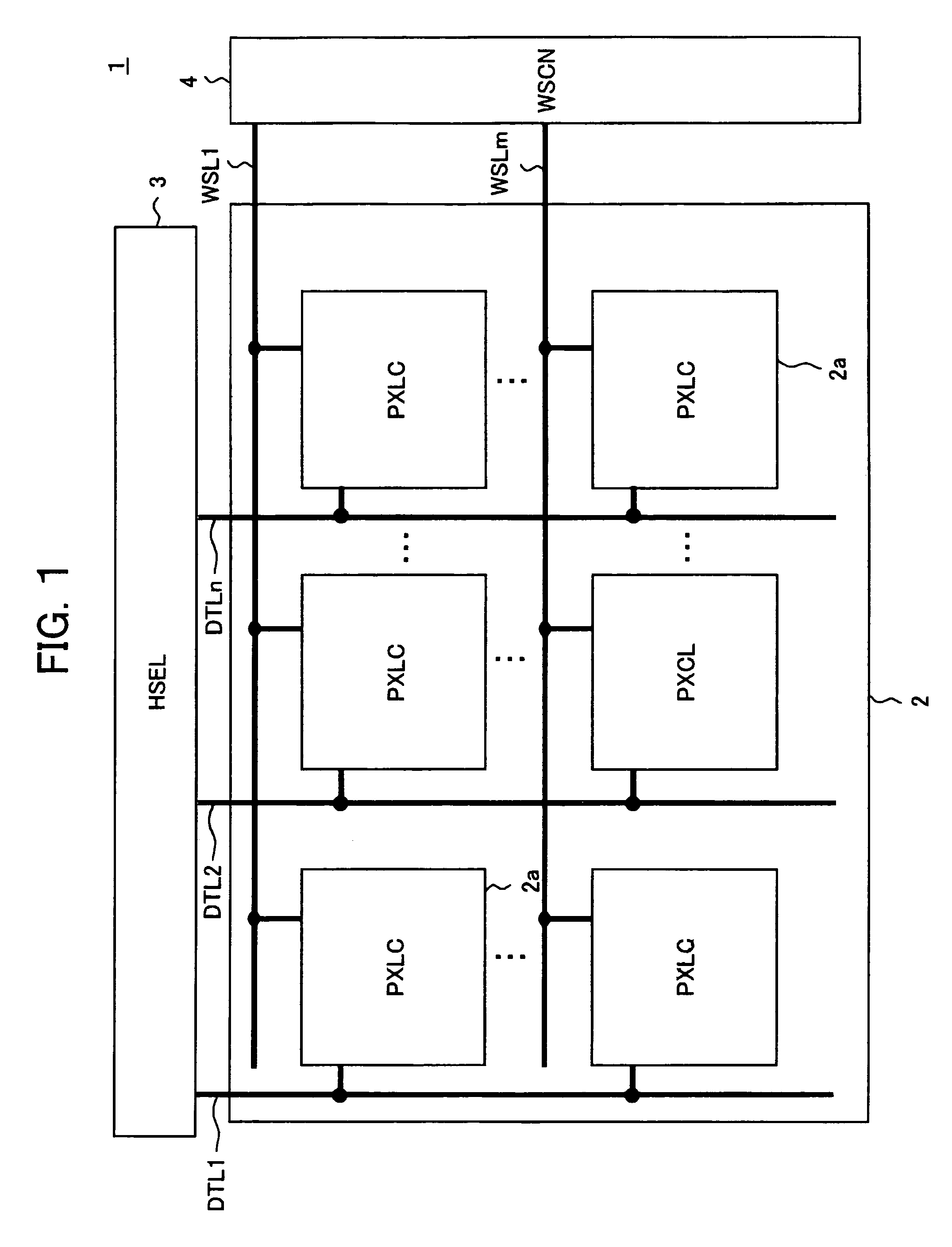
[0131]This display device 100, as shown in FIG. 8 and FIG. 9, has a pixel array 102 comprised of pixel circuits (PXLC) 101 arranged in an m×n matrix, horizontal selector (HSEL) 103, write scanner (WSCN) 104, first drive scanner (DSCN1) 105, second drive scanner (DSCN2) 106, third drive scanner (DSCN3) 107, fourth drive scanner (DSCN4) 108, fifth drive scanner (DSCN5) 109, sixth drive scanner (DSCN6) 110, reference constant current source (RCIS) 111, data lines DTL101 to DTL10n selected by the horizontal selector 103 and supplied with data signals in accordance with the luminance information, scanning lines WSL101 to WSL10m selected and driven by the write scanner 104, drive l...

second embodiment

[0189]FIG. 19 is a circuit diagram showing the specific configuration of a pixel circuit according to a second embodiment. Further, FIG. 20 is a timing chart of the circuit of FIG. 19.

[0190]The difference of the second embodiment from the first embodiment explained above resides in that the fourth switch constituted by the TFT 115 does not share the predetermined potential line to which the TFT 115 is connected together with the data line DTL, but is separately provided.

[0191]The rest of the configuration is the same as that of the first embodiment, so a detailed explanation concerning the configuration and function is omitted here.

[0192]In the second embodiment, when running the reference current Iref to the source of the driver transistor constituted by the TFT 111, the input voltage Vin is not input to the gate voltage of the TFT 111, but the fixed potential V0 is input. By inputting the fixed potential V0 and running the reference current Iref, the time during which the Vin is i...

third embodiment

[0194]FIG. 21 is a block diagram showing the configuration of an organic EL display device employing a pixel circuit according to a third embodiment.

[0195]FIG. 22 is a circuit diagram showing the specific configuration of a pixel circuit according to the third embodiment in the organic EL display device of FIG. 21. Further, FIGS. 23A to 23H are timing charts of the circuit of FIG. 22.

[0196]The difference of the third embodiment from the first embodiment resides in that, in place of the configuration in which the electric connecting means for connecting the first electrode of the capacitor C112 and the second node ND112 is configured by the switch 118 for selectively connecting the two, they are directly connected by an electric interconnect.

[0197]As a result, the third drive scanner 107 and the drive line DSL121 become unnecessary.

[0198]The rest of the configuration is the same as that of the second embodiment explained above.

[0199]According to the third embodiment, in addition to t...


PUM


Abstract

A pixel circuit, a display device, and a method of driving a pixel circuit able to obtain a source-follower output without luminance deterioration even when the current-voltage characteristic of a light emitting element changes due to aging, making a source-follower circuit of n-channel transistors possible, and in addition able to display uniform and high quality images not without regard to variations of threshold values and mobilities of the active elements inside pixels, wherein a capacitor C111 is connected between a gate and a source of a TFT 111, the source side of the TFT 111 is connected to a fixed potential (GND) through a TFT 114, a predetermined reference current Iref is supplied to the source of the TFT 111 with a predetermined timing, a voltage corresponding to the reference current Iref is held, and an input signal voltage centered about the voltage is coupled, whereby an EL light emitting element 19 is driven centered about the center value of variation of the mobilities.

Description

TECHNICAL FIELD[0001]The present invention relates to a pixel circuit having an electro-optical element controlled in luminance by a current value in an organic EL (electroluminescence) display etc., and more particularly, among image display devices in which these pixel circuits are arranged in a matrix, to a so-called active matrix type image display device in which the value of the current flowing in each electro-optical element is controlled by an insulating gate type field effect transistor provided inside each pixel circuit, and a method of driving the pixel circuit.BACKGROUND ART[0002]In an image display device, for example, a liquid crystal display etc., the image is displayed by arranging a large number of pixels in a matrix and controlling the intensity of light for each pixel in accordance with image information to be displayed.[0003]The same is also true for an organic EL display etc., but an organic EL display is a so-called self light emission type display having a lig...

Claims


Application Information

Patent Timeline
Patent Type & Authority Patents(United States)
IPC IPC(8): G09G3/30H01L51/50G09F9/30G09G3/20G09G3/32G09G5/10H01L29/786H05B33/00H05B33/14
CPCG09G3/3233G09G2300/0819G09G2320/043G09G2300/0861G09G2310/0262G09G2300/0852G09G3/20G09G3/30
Inventor UCHINO, KATSUHIDEYAMASHITA, JUNICHIYAMAMOTO, TETUROU
Owner SONY CORP
Why Eureka
Try Eureka