Organic electroluminescence device

a technology of electroluminescence device and organic el, which is applied in the direction of solid-state devices, electric lighting sources, and light sources. it can solve the problems of reducing the yield of organic el products, difficult to handle, and the driving voltage of a phosphorescence organic el device with a high quantum efficiency of light emission is higher, and achieves stable life and high temperature preservation without luminance degradation

Active Publication Date: 2011-07-14
PIONEER CORP
View PDF1 Cites 10 Cited by
  • Summary
  • Abstract
  • Description
  • Claims
  • Application Information

AI Technical Summary

Benefits of technology

Accordingly, there is one of exemplary tasks to be achieved by the present invention to provide an organic electroluminescence device comprising an n-type-dopant-containing electron transport layer and capable of being life-prolonged stably in a long-range storage and a high temperature preservation without luminance deterioration.

Problems solved by technology

There is a problem that a driving voltage of a phosphorescence organic EL device with a high quantum efficiency of light emission is higher than that of a fluorescence organic EL device.
In this case there is increase in occurrence of defective electricity between the electrodes i.e., anode and cathode of the device, resulting in decrease of yields on products of the organic EL devices.
However, since these alkaline metal and alkaline earth metal have deliquescence and absorbency, it is difficult to handle them.
Especially alkaline metal and alkaline earth metal such as metal cesium etc. having a low work function exhibit a high doping efficiency, but it is very dangerous to deal with the metal cesium in the air due to instability thereof.

Method used


Image

  • Organic electroluminescence device
  • Organic electroluminescence device
  • Organic electroluminescence device

Examples


embodiment 3

For Embodiment 3, plural organic EL devices were fabricated using an n-type-dopant-containing electron transport layer containing another n-type dopant.

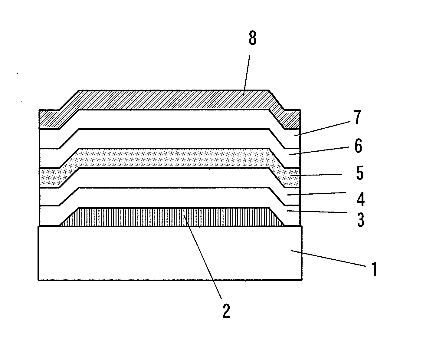
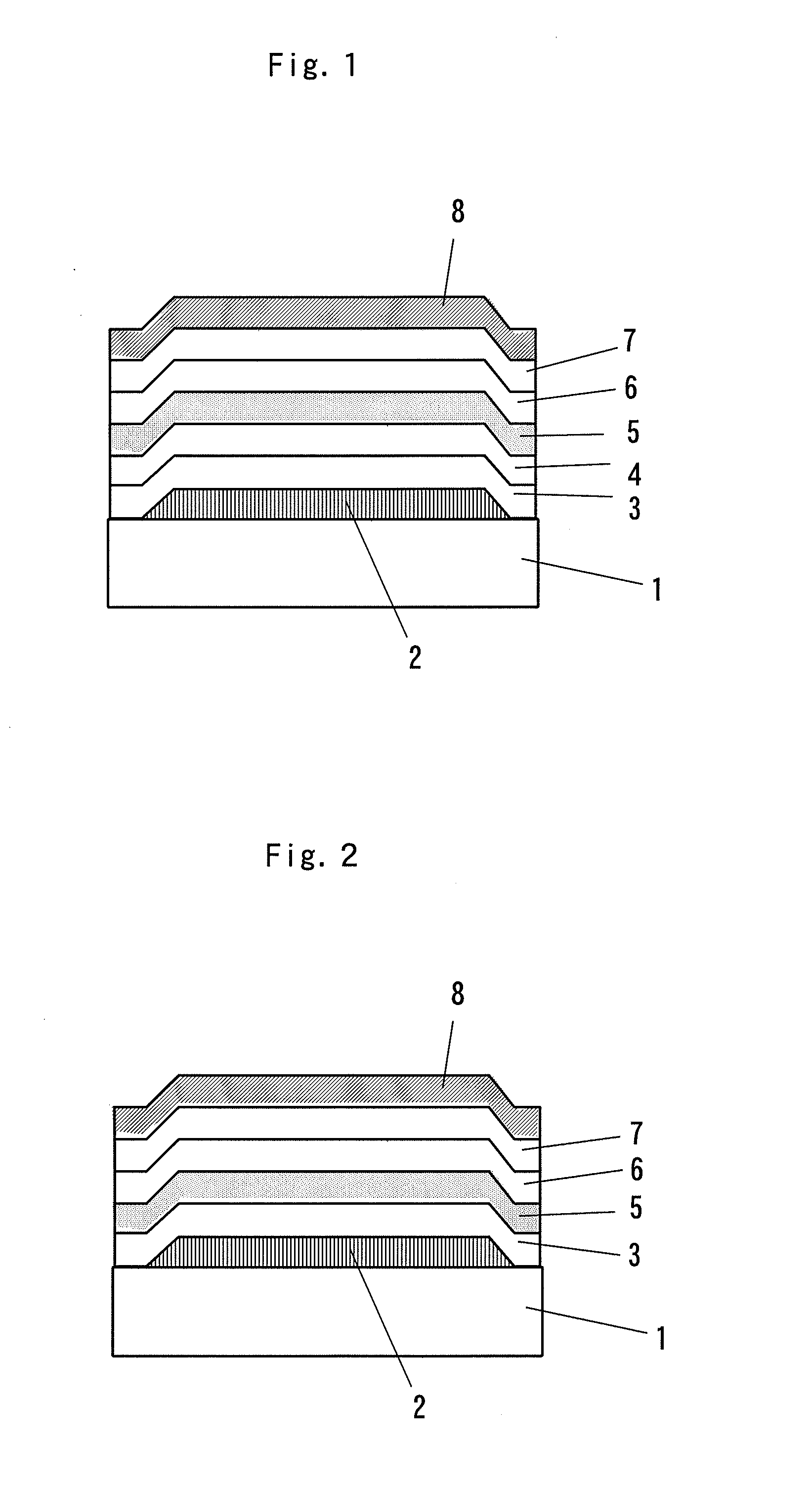
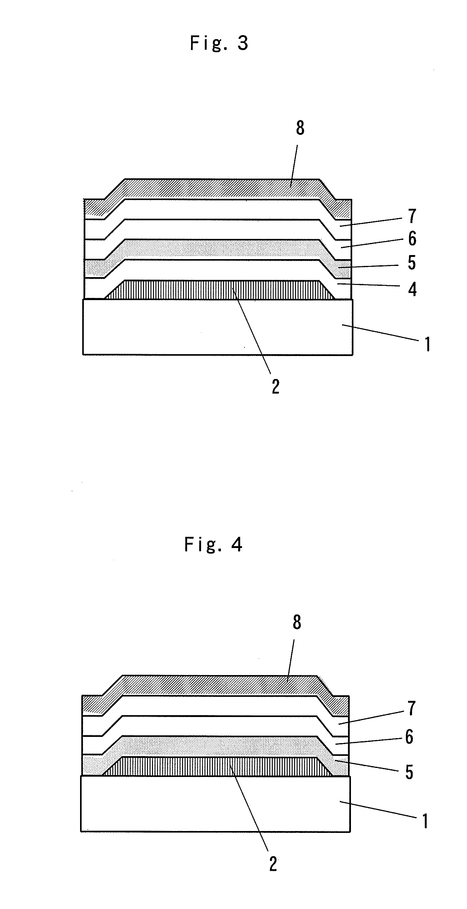
Plural organic EL devices of Embodiments 3 were fabricated in the same manner as Embodiments 1, except that n-type-dopant blocking layers made of Ir(ppy)3 at 100 vol % and n-type-dopant-containing electron transport layers of the n-type dopant of tungstate Cs2WO4 instead of the molybdate Cs2MoO4 were layered respectively. The device structure of Embodiment 3 has, in order of ITO / hole injection layer / hole transport layer / light-emitting layer / n-type-dopant blocking layer / electron transport layer / Al, ITO / CuPc(25) / NPB(40) / Ir(ppy)3-9 vol %: TRZ(40) / 1.7 vol %-Cs2WO4:NBphen(20) / Al. Here, the content in the last parentheses ( ) in each layer section denotes a thickness (nm).

Plural organic EL devices of Comparative examples 3 were fabricated in the same manner as Comparative examples 2, except that the n-type dopant of tungstate was used for ...

embodiments 4 and 5

For other Embodiments, plural organic EL devices were fabricated using an n-type-dopant blocking layer serving as a light-emitting layer unified in one piece so as to be an n-type dopant-blocking light-emitting layer having an increased thickness.

A plurality of organic EL devices (Embodiment 4) were fabricated in such a manner that each organic EL device included an n-type-dopant-containing electron transport layer (in which an organic compound capable of transporting electrons of NBphen as a first component was mixed with an n-type dopant Cs2MoO4 containing Cs of alkaline metal as an electron donor of a second component) and an n-type-dopant blocking light-emitting layer (in which an organic compound capable of transporting electrons of TRZ (host material) as a third component was mixed with a heavy atom compound of Ir(ppy)3 containing at least one kind of heavy atoms with an atomic weight of 79 or more as a fourth component (phosphorescence guest material)). Then some characterist...


PUM


Abstract

An organic electroluminescence device includes a plurality of organic semiconductor layers including an organic light-emitting layer and layered or disposed between a pair of anode and cathode opposed to each other. The device includes n-type-dopant-containing electron transport layer disposed between the cathode and the organic light-emitting layer. The n-type-dopant-containing electron transport layer includes an organic compound capable of transporting electrons as a first component which mixed with an n-type dopant of an electron donor of metallic atom or ion thereof as a second component. The organic electroluminescence device further includes an n-type-dopant blocking layer having an interface contacting with the n-type-dopant-containing electron transport layer to block the n-type dopant. The n-type-dopant blocking layer includes a heavy atom compound including at least one kind of heavy atoms with an atomic weight of 79 or more.

Description

TECHNICAL FIELDThe present invention relates to organic electroluminescence devices and particularly to an organic electroluminescence (abbreviated as EL) device utilizing organic compounds having electric charge-transporting properties (hole and / or electron mobility) and comprising an organic light-emitting layer made of such an organic compound thereof.BACKGROUND ARTConventionally, the organic EL films of an organic EL device have a lamination structure of a plurality of layered organic material layers. The organic material layers includes an organic light-emitting layer and also a material layer having a hole-transporting capability such as a hole injection layer, a hole transport layer or the like, as well as a material layer having an electron transporting capability such as an electron transport layer, an electron injection layer or the like. The electron injection layer may include an inorganic compound such as alkaline metal, alkaline earth metal or a compound which contains...

Claims


Application Information

Patent Timeline
Patent Type & Authority Applications(United States)
IPC IPC(8): H01L51/50
CPCH01L51/0085H01L51/5052H01L51/0087H10K85/346H10K85/342H10K50/165H05B33/18H10K50/81H10K50/805H10K50/82H10K50/85H10K2102/302
Inventor OYAMADA, TAKAHITOTSUJI, TAISHITAKAHASHI, YASUHIRO
Owner PIONEER CORP
Why Eureka
Try Eureka