Electronic component with shielding case and method of manufacturing the same

a technology of electronic components and shielding cases, which is applied in the direction of printed element electric connection formation, electric apparatus casings/cabinets/drawers, generators/motors, etc., can solve the problems of increasing cost and reducing so as to reduce the cost and increase the available area of motherboards , the effect of increasing the available area of motherboards

Active Publication Date: 2008-04-22
MURATA MFG CO LTD
View PDF19 Cites 13 Cited by
  • Summary
  • Abstract
  • Description
  • Claims
  • Application Information

AI Technical Summary

Benefits of technology

[0010]In order to overcome the problems described above, preferred embodiments of the present invention provide methods of manufacturing electronic components with shielding cases leading to an increase in the available area of a motherboard, a reduction in cost, and downsizing of the electronic components, and preferred embodiments of the present invention also provide an electronic component with a shielding case produced by the novel methods of other preferred embodiments of the present invention.

Problems solved by technology

This leads to a reduction in the available area of the motherboard and an increase in cost.

Method used


Image

  • Electronic component with shielding case and method of manufacturing the same
  • Electronic component with shielding case and method of manufacturing the same
  • Electronic component with shielding case and method of manufacturing the same

Examples


first preferred embodiment

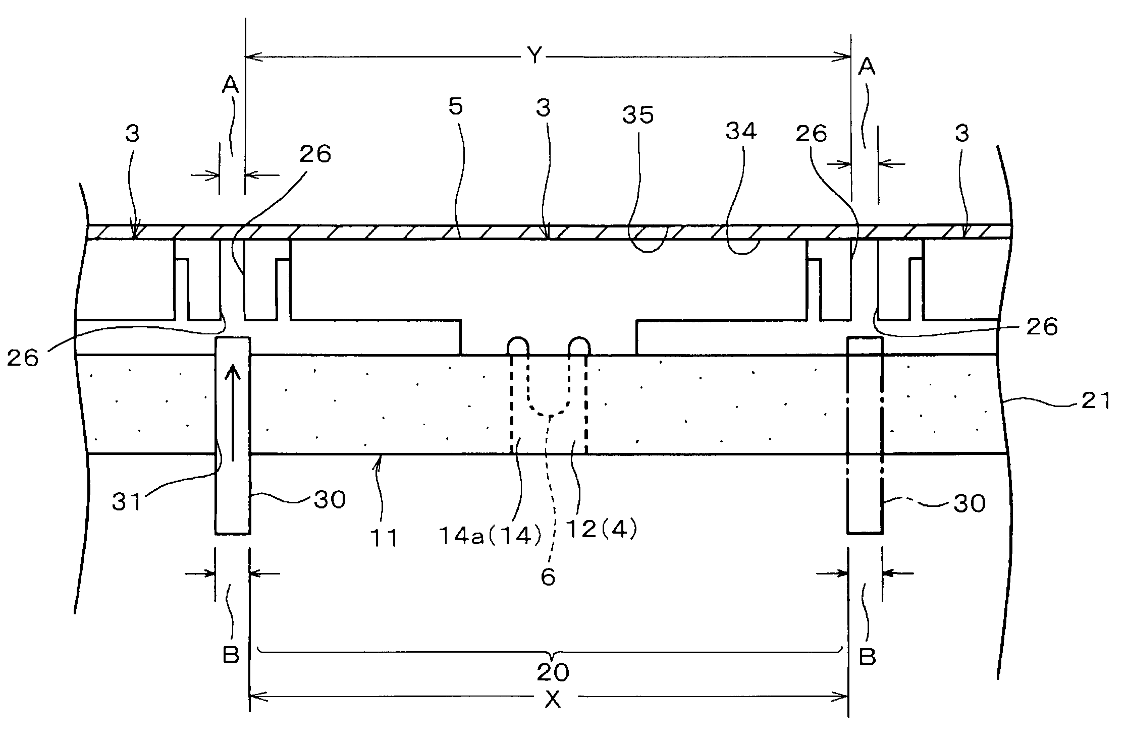
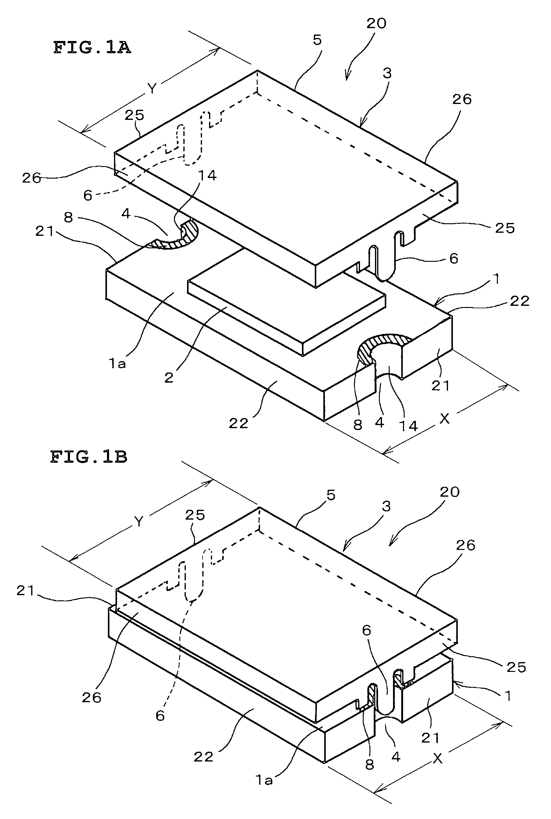
[0031]With reference to FIG. 1A, an electronic component 20 with a shielding case according to a first preferred embodiment of the present invention preferably includes a substrate 1, a surface mount device (circuit module) 2 mounted on the top surface 1a of the substrate 1, and a shielding case 3 composed of a conductive material and accommodating the substrate 1 and the surface mount device 2.

[0032]The substrate 1 is preferably a substantially rectangular plate including a pair of opposed first side surfaces 21 each having a catching groove 4 for mounting the shielding case 3, and a pair of second side surfaces 22 each having no grooves.

[0033]The shielding case 3 is preferably substantially rectangular when viewed from the top, and includes a casing body 5 covering the top surface 1a of the substrate 1. The casing body 5 includes a pair of opposed first surfaces 25, catching pieces 6 each protruding from the first surfaces 25 for engaging with the catching grooves 4 of the substra...

second preferred embodiment

[0044]FIG. 5 is a cross-sectional view illustrating a step of dividing a motherboard in a method of manufacturing electronic components with shielding cases according to a second preferred embodiment of the present invention. In FIG. 5, elements having the same reference numerals or symbols as in FIG. 3 are identical or corresponding to those in FIG. 3.

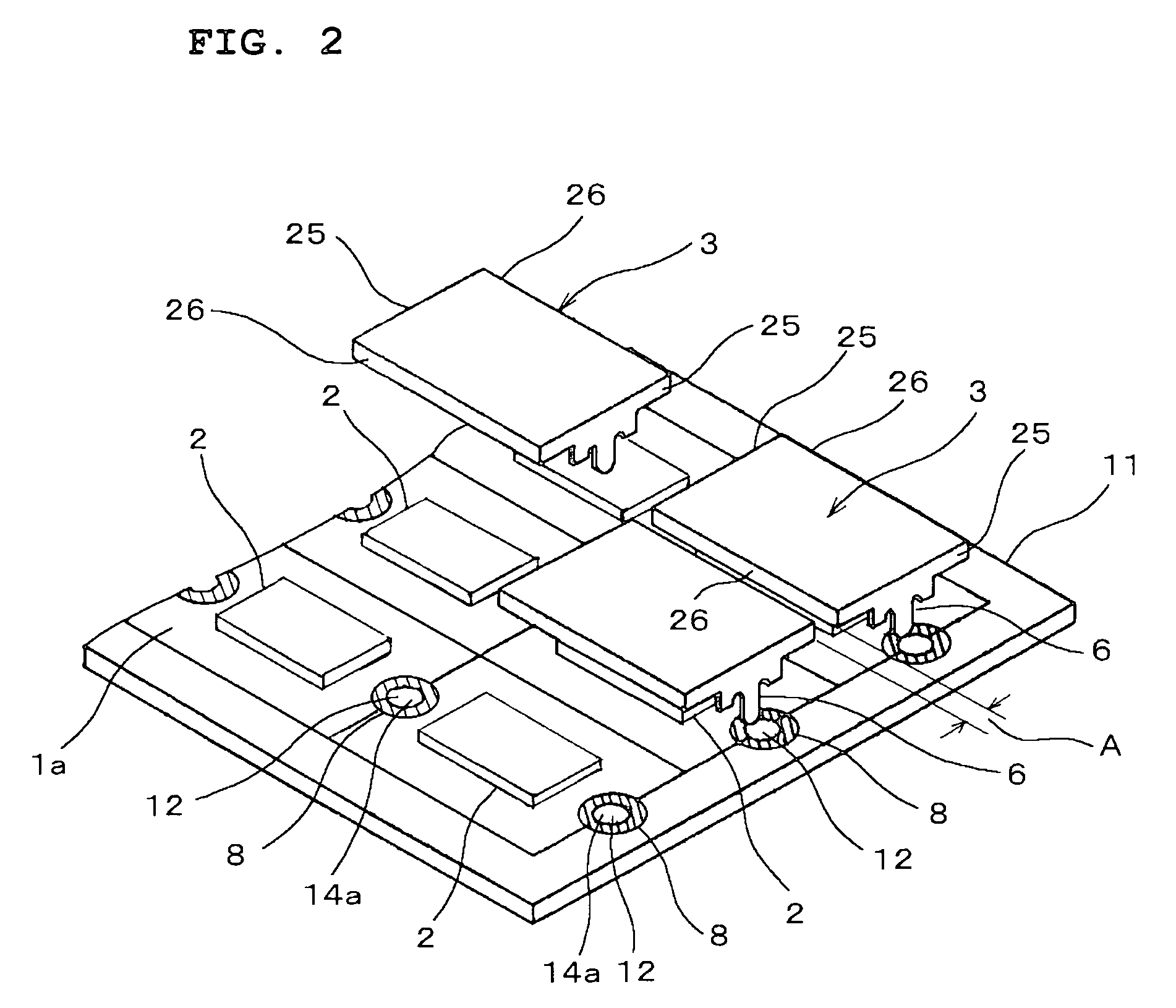
[0045]In the second preferred embodiment, a shielding-case array 33 of shielding cases 3 connected to each other is used. After the shielding-case array 33 is mounted on a motherboard 11, the motherboard 11 is cut with a dicing blade 30 such that the dicing blade 30 reaches connecting portions 40 that connect the shielding cases 3 in the cutting step of the motherboard 11. In this manner, the connecting portions 40 and the motherboard 11 are cut with the dicing blade 30 at the same time.

[0046]As described above, by cutting the connecting portions 40 of the shielding-case array 33 at the same time as the division of the motherboard 11,...


PUM

PropertyMeasurementUnit
depthaaaaaaaaaa
widthsaaaaaaaaaa
thicknessaaaaaaaaaa

Abstract

Shielding cases each include a pair of opposed first surfaces with catching pieces protruding therefrom and a pair of second surfaces without catching pieces. A motherboard forms substrates each including a pair of opposed first side surfaces with catching grooves and a pair of second side surfaces without catching grooves when it is divided. The shielding cases are mounted on the motherboard such that the intervals A between the second surfaces of two adjacent shielding cases are equal to or less than the widths B of cutting allowances for cutting the motherboard. The motherboard is cut from the opposite side of a surface of the motherboard on which the shielding cases are mounted at predetermined positions where the second side surfaces are formed on each substrate. In this manner, the motherboard is divided into electronic components with shielding cases.

Description

BACKGROUND OF THE INVENTION[0001]1. Field of the Invention[0002]The present invention relates to electronic components. In particular, the present invention relates to electronic components with shielding cases accommodating surface mount devices mounted on the substrates in the same manner as high-frequency composite components such as voltage controlled oscillators (VOCs) or phase-locked loop (PLL) modules, and relates to methods of manufacturing the same.[0003]2. Description of the Related Art[0004]FIG. 6 is a perspective view of a known electronic component with a shielding case (See Japanese Unexamined Patent Application Publication No. 2001-148594). This electronic component includes a substrate 51, a surface mount device (not shown) mounted on the top surface 51a of the substrate 51, and a shielding case 53 accommodating the substrate 51 and the surface mount device.[0005]The substrate 51 includes four side surfaces each having a plurality of catching grooves 54 for mounting ...

Claims


Application Information

Patent Timeline
Patent Type & Authority Patents(United States)
IPC IPC(8): H05K7/02H05K9/00H05K3/00H05K3/34H05K3/40H05K5/04H05K13/00
CPCH05K3/3405H05K9/0028H05K3/0052H05K3/403Y10T29/49126H05K2201/09181H05K2201/10371
Inventor MASHIMO, YOSHIYUKIUNO, MASAOYAOEDA, TORU
Owner MURATA MFG CO LTD
Why Eureka
Try Eureka