Self-healing chip-to-chip interface

a chip-to-chip interface and self-healing technology, applied in the field of data processing systems, can solve the problems of scrapping or dumping of components identified with defects, such as non-functional signal paths, and increasing the number of interconnections between integrated circuits

Inactive Publication Date: 2008-04-22
INT BUSINESS MASCH CORP
View PDF28 Cites 89 Cited by
  • Summary
  • Abstract
  • Description
  • Claims
  • Application Information

AI Technical Summary

Problems solved by technology

As computer systems become increasingly more complex, the number of interconnections between integrated circuits also increases.
The defective or failing component often causes part or all of the computer system to be unavailable.
Further, during testing and manufacturing of components, any components identified with defects, such as a non-functional signal path, are scrapped or discarded.
The yields of usable components are often very low.

Method used


Image

  • Self-healing chip-to-chip interface
  • Self-healing chip-to-chip interface
  • Self-healing chip-to-chip interface

Examples


Embodiment Construction

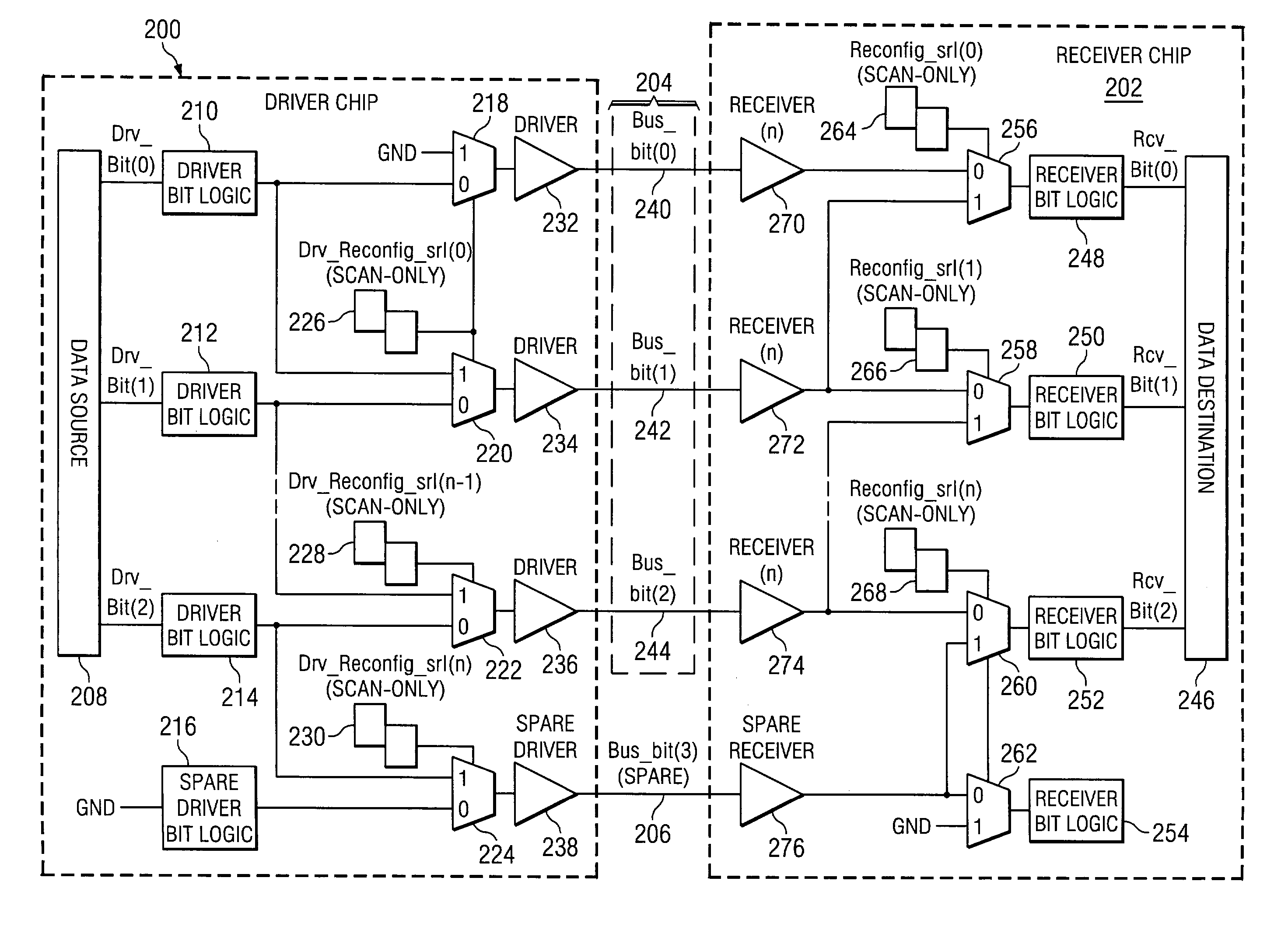
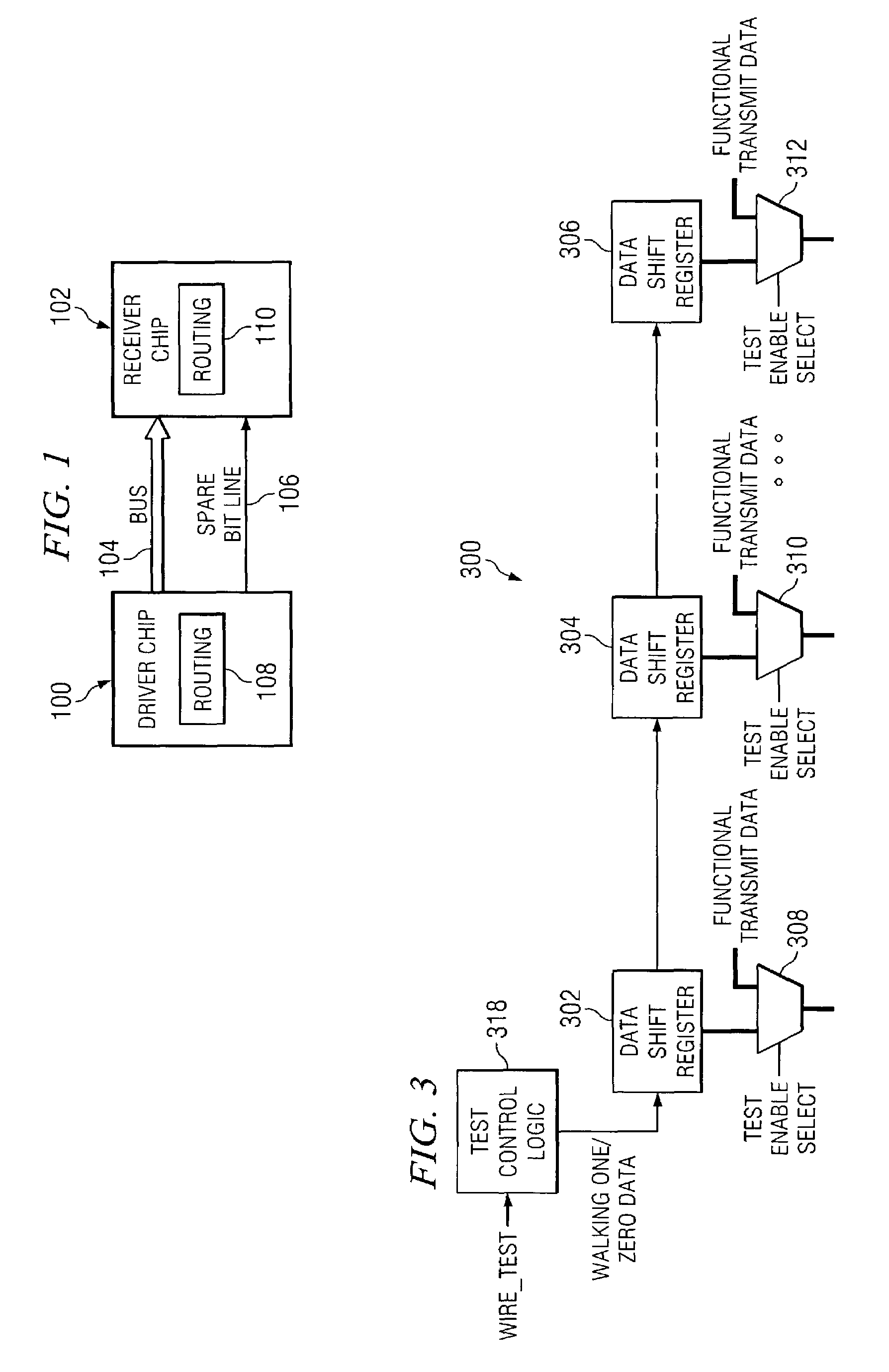
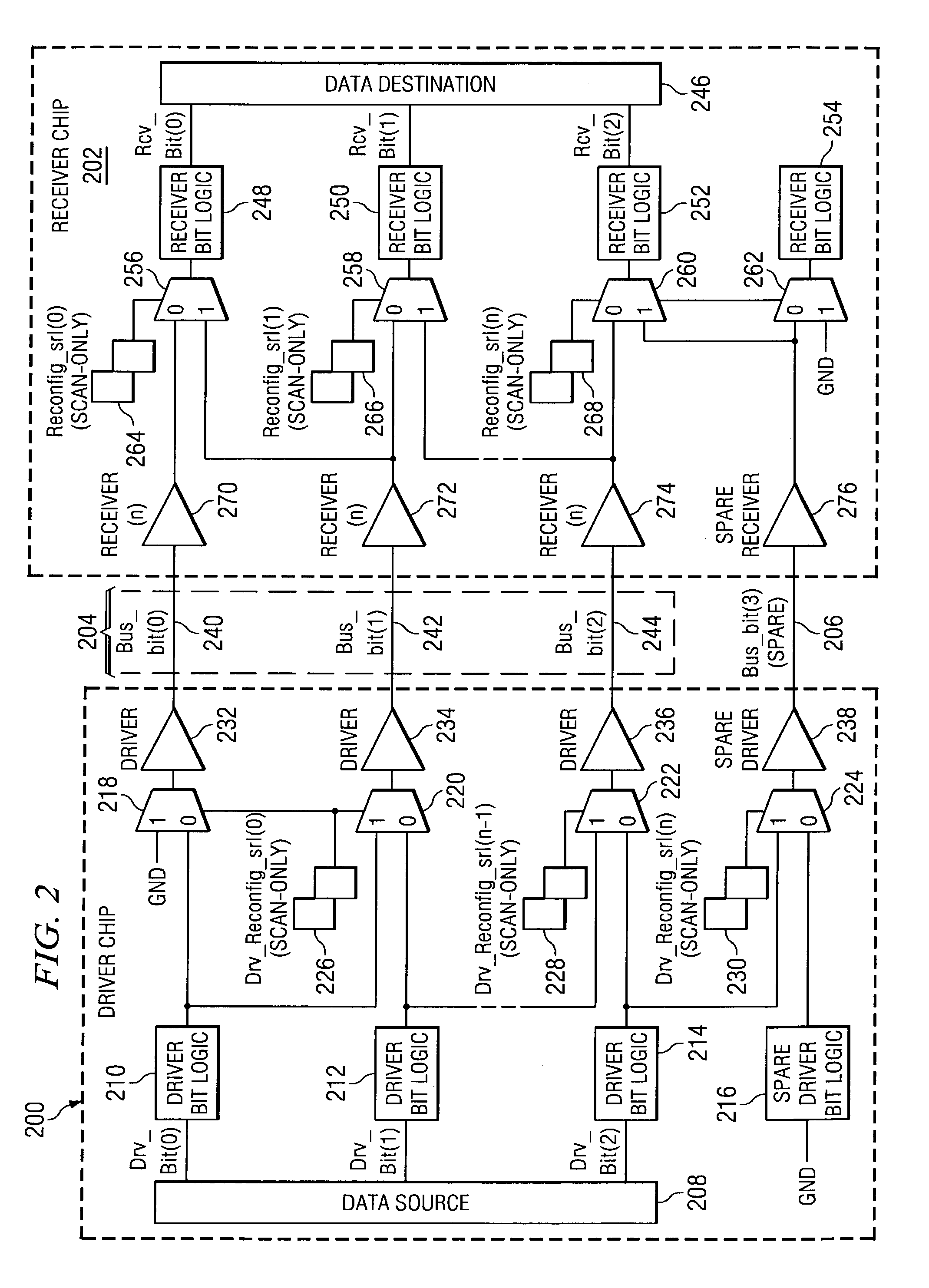
[0016]With reference now to the figures, and in particular to FIG. 1, a diagram illustrating chips with a self-healing interface is depicted in accordance with a preferred embodiment of the present invention. In this example, driver chip 100 sends signals to receiver chip 102 over bus 104. A bus is a common pathway or channel providing a connection between devices. Bus 104 provides a path for signals to travel between driver chip 100 and receiver chip 102. Additionally, spare bit line 106 also provides a connection between driver chip 100 and receiver chip 102.

[0017]The mechanism of the present invention employs routing 108 and routing 110 to manage or handle a defective signal path or a failure in a signal path within bus 104. These routing mechanisms, routing 108 and routing 110, allow for driver chip 100 and receiver chip 102 to repair themselves to allow signal paths to be dynamically reconfigured. Such a mechanism allows for defects to exist in the bus while still maintaining o...


PUM


Abstract

A method, apparatus, and computer instructions for managing a set of signal paths for a chip. A defective signal path within the set of signal paths for the chip is detected. Signals are re-routed through the set of signal paths such that the defective signal path is removed from the set of signal paths and sending signals using remaining data signal paths in the set of signal paths and using an extra signal path in response to detecting the defective signal path.

Description

BACKGROUND OF THE INVENTION[0001]1. Technical Field[0002]The present invention relates generally to an improved data processing system, and in particular, to a method and apparatus for routing data. Still more particularly, the present invention provides a method and apparatus for routing data between chips across a bus.[0003]2. Description of Related Art[0004]As computer systems become increasingly more complex, the number of interconnections between integrated circuits also increases. The number of interconnections between chips, such as microprocessors, memory, and input / output chips is increasing to numbers, such as tens of thousands of interconnections between chips in a computer system. All of these signals sent between different components pass through a chip's package or module, a board, and possibly across a connector to another board and then to another module arriving at a final destination. All of these signal paths are required to be manufactured and remain defect free ...

Claims


Application Information

Patent Timeline
Patent Type & Authority Patents(United States)
IPC IPC(8): G01R31/08G06F13/00G06F11/26H01L21/66
CPCH01L22/22H01L2924/0002H01L2924/00G06F11/26
Inventor BECKER, WIREN DALEDREPS, DANIEL MARKFERRAIOLO, FRANK DAVIDHARIDASS, ANANDREESE, ROBERT JAMES
Owner INT BUSINESS MASCH CORP
Why Eureka
Try Eureka