Method for forming high reliability bump structure

Active Publication Date: 2008-04-29
TAIWAN SEMICON MFG CO LTD
View PDF5 Cites 38 Cited by
  • Summary
  • Abstract
  • Description
  • Claims
  • Application Information

AI Technical Summary

Problems solved by technology

As semiconductor device sizes have decreased, the density of devices on a chip has increased along with the size of the chip thereby making chip bonding more challenging.
One of the major problems leading to package failure as chip sizes increase is the increasing difficult problem of coefficient of thermal expansion (

Method used


Image

  • Method for forming high reliability bump structure
  • Method for forming high reliability bump structure
  • Method for forming high reliability bump structure

Examples


Embodiment Construction

[0015]In the following description, numerous specific details are set forth to provide a thorough understanding of the present invention. However, one having an ordinary skill in the art will recognize that the invention can be practiced without these specific details. In some instances, well-known processes and structures have not been described in detail to avoid unnecessarily obscuring the present invention.

[0016]Reference will now be made in detail to the present preferred embodiments of the present invention, examples of which are illustrated in the accompanying drawings.

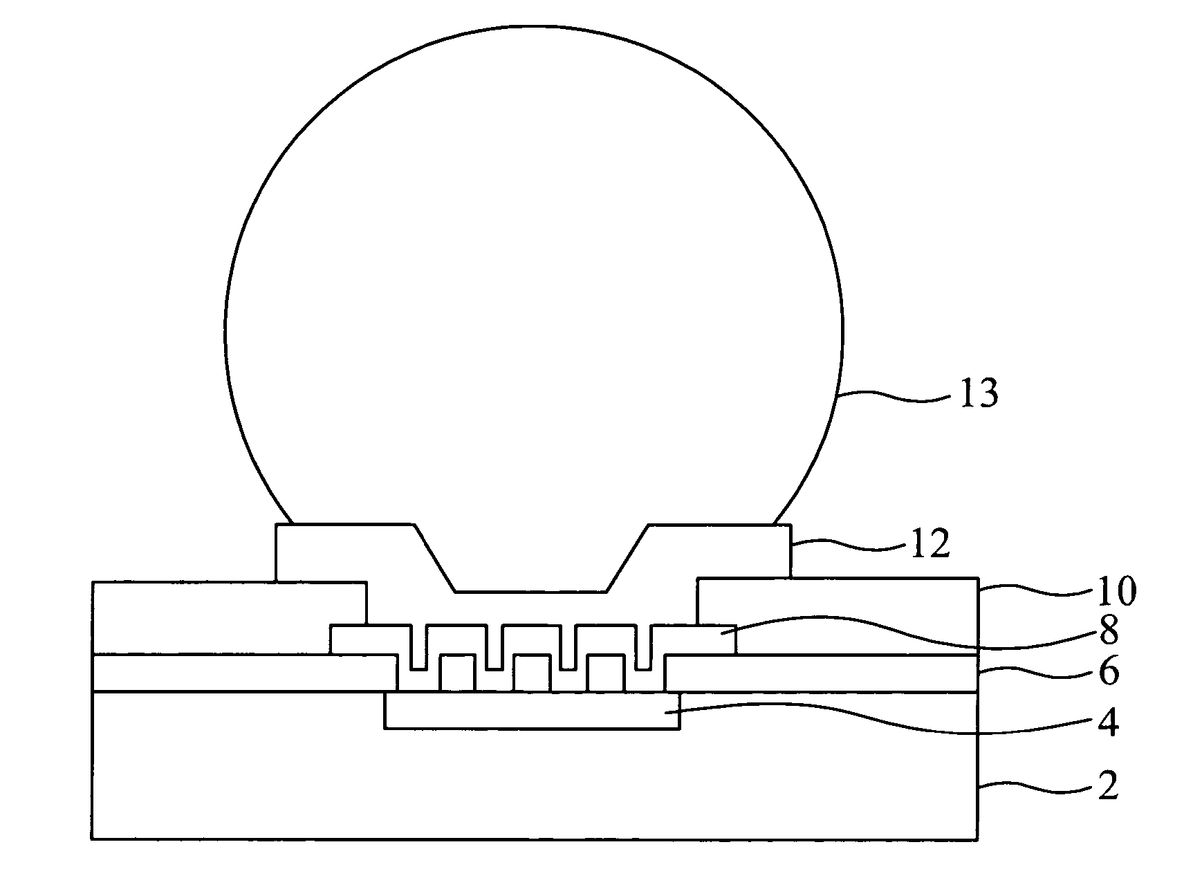
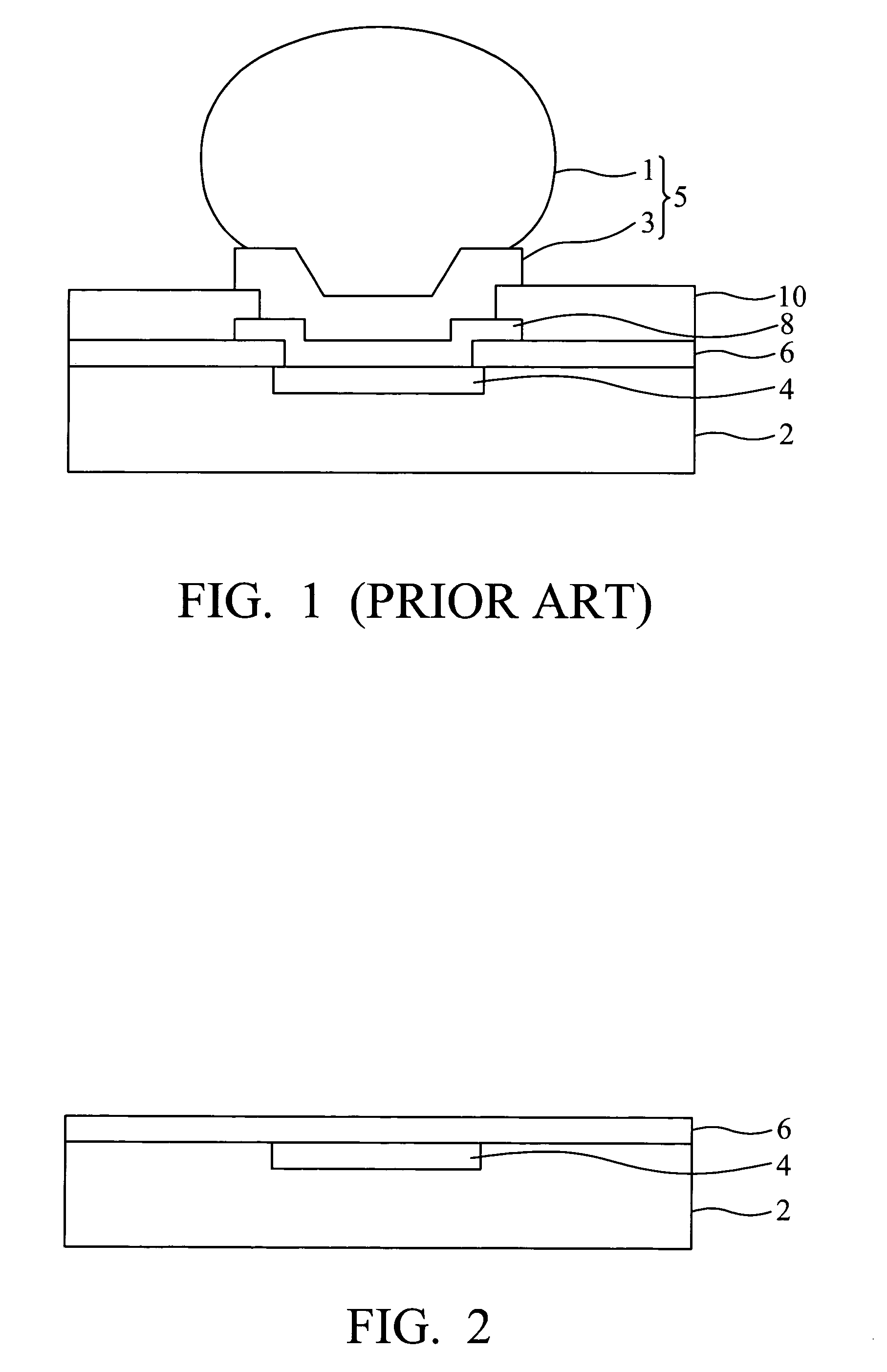
[0017]FIGS. 2-11 are cross-sectional views of a semiconductor device depicting a method of forming a solder bump according to one embodiment of the present invention. As shown in FIG. 2, a semiconductor substrate 2 is provided having a top metal layer 4 therein, Substrate 2 is understood to include active and passive devices, conductive layers and dielectric layers and the type of the substrate is a design choi...


PUM


Abstract

Methods for forming a bump on a semiconductor substrate, the substrate having a contact pad thereon, is provided. In one embodiment, the method comprises depositing a passivation layer over the substrate and the contact pad. The passivation layer is patterned and etched to form a plurality of openings in the passivation layer exposing portions of the contact pad. An under bump metallurgy (UBM) layer is deposited over the etched passivation layer and in the plurality of openings thereof to contact the contact pad. A photoresist layer is formed on the UBM layer and then patterned and etched to form at least one opening substantially overlying the contact pad. An electrically conductive material is deposited into the opening formed in the photoresist layer and overlying the UBM layer and aligned with the contact pad. A portion of the remaining photoresist layer is removed. The UBM layer is etched using the electrically conductive material as a mask. Thereafter, the electrically conductive material is reflowed to provide a bump on the semiconductor substrate.

Description

BACKGROUND OF THE INVENTION[0001]1. Field of the Invention[0002]The present invention relates generally to the fabrication of solder bumps for the interconnection of semiconductor devices, and more particularly, to under bump metallurgy (UBM) layers that have improved adhesion properties.[0003]2. Brief Discussion of the Related Art[0004]As semiconductor device sizes have decreased, the density of devices on a chip has increased along with the size of the chip thereby making chip bonding more challenging. One of the major problems leading to package failure as chip sizes increase is the increasing difficult problem of coefficient of thermal expansion (CTE) mismatches between materials leading to thermal and mechanical stress buildup and consequent failure. For example, in flip chip technology, chip bonding is accomplished by means of solder bumps formed on under bump metallurgy (UBM) layers overlying a chip contact pad. Frequently, improper bonding between the solder bump and the UBM...

Claims


Application Information

Patent Timeline
IPC IPC(8): H01L21/44H01L23/48H01L23/52H01L29/40
CPCH01L24/03H01L24/05H01L2924/0002H01L2224/0554H01L2224/05572H01L2224/05001H01L2224/05559H01L24/11H01L2224/03912H01L2224/0401H01L2224/1147H01L2924/01013H01L2924/01014H01L2924/01029H01L2924/0105H01L2924/01078H01L2924/01082H01L2924/014H01L2924/05042H01L2924/14H01L2924/01033H01L2224/05027H01L2224/05017H01L2924/00014H01L2924/00012H01L2224/05552H01L2224/05556
Inventor CHIU, SUNG-CHENGTSAI, HAO-YIYU, HSIU-MEICHEN, SHIH-MINGHOU, SHANG-YUN
Owner TAIWAN SEMICON MFG CO LTD
Why Eureka
Try Eureka