
Non-volatile programmable memory cell and array for programmable logic array

a programmable logic array and non-volatile technology, applied in the direction of electrical equipment, semiconductor devices, instruments, etc., can solve the problem of not decreasing the voltage used to program and erase non-volatile memory transistors

Active Publication Date: 2008-05-06
MICROSEMI SOC
View PDF5 Cites 59 Cited by
  • Summary
  • Abstract
  • Description
  • Claims
  • Application Information

AI Technical Summary

Problems solved by technology

This presents a problem in that the voltages used to program and erase non-volatile memory transistors are not decreasing as fast as the voltages that are used to operate the transistors from which the logic is configured.

Method used


Image

  • Non-volatile programmable memory cell and array for programmable logic array
  • Non-volatile programmable memory cell and array for programmable logic array
  • Non-volatile programmable memory cell and array for programmable logic array

Examples


Embodiment Construction

[0015]Persons of ordinary skill in the art will realize that the following description of the present invention is illustrative only and not in any way limiting. Other embodiments of the invention will readily suggest themselves to such skilled persons.

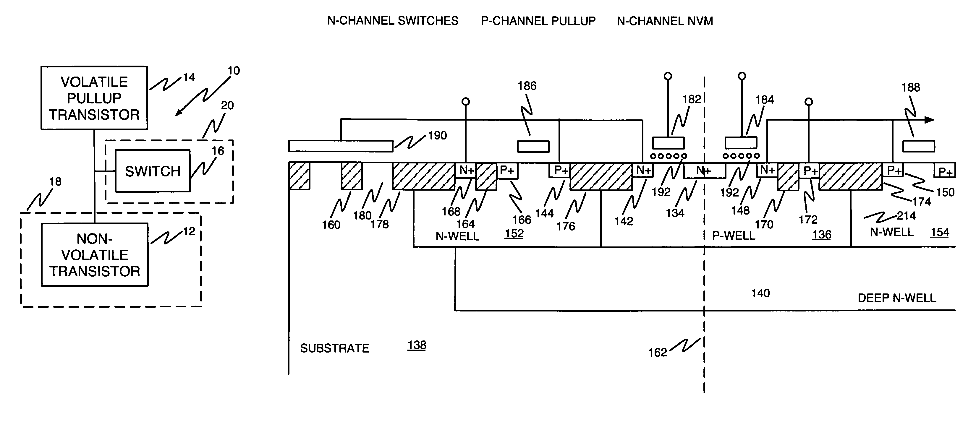
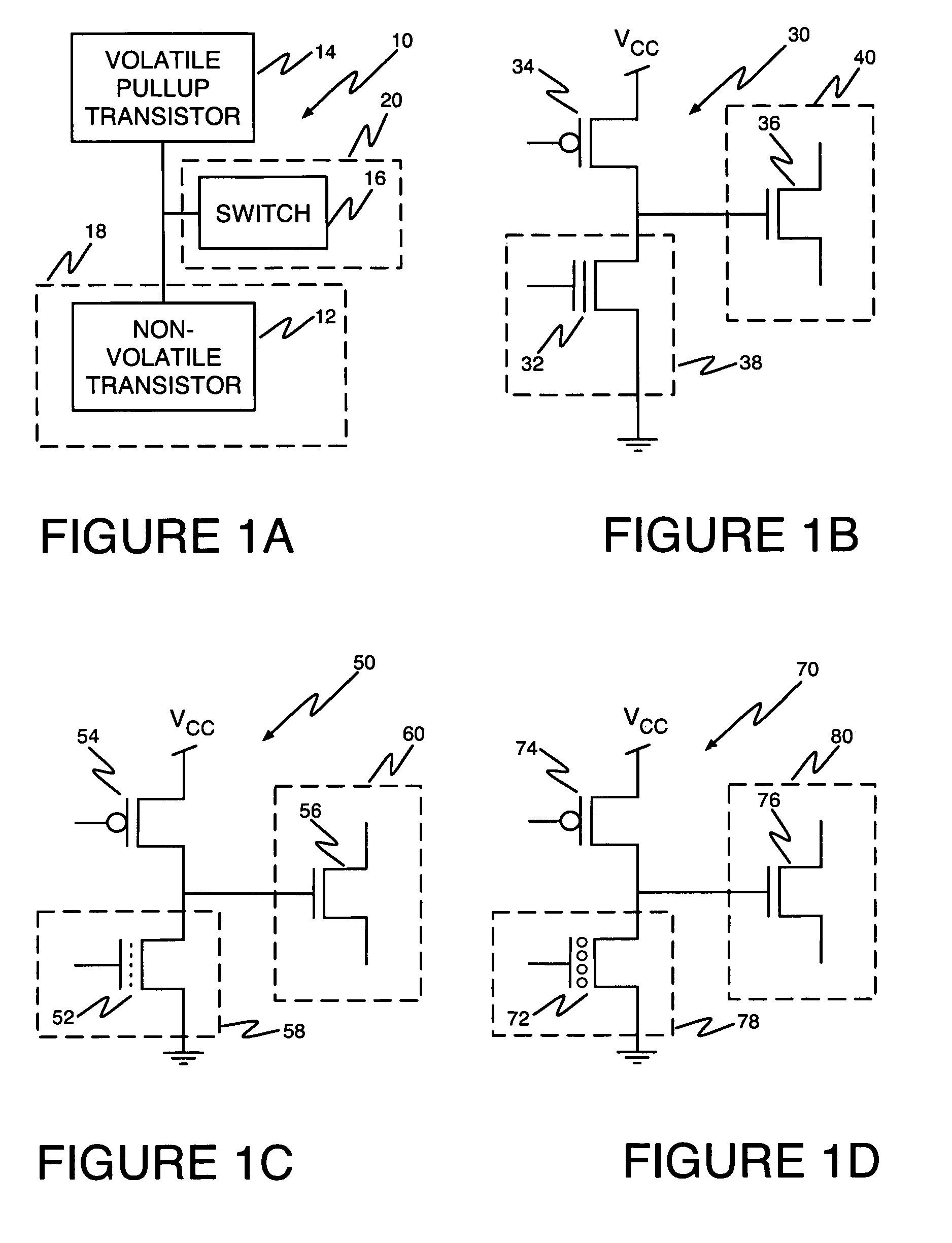
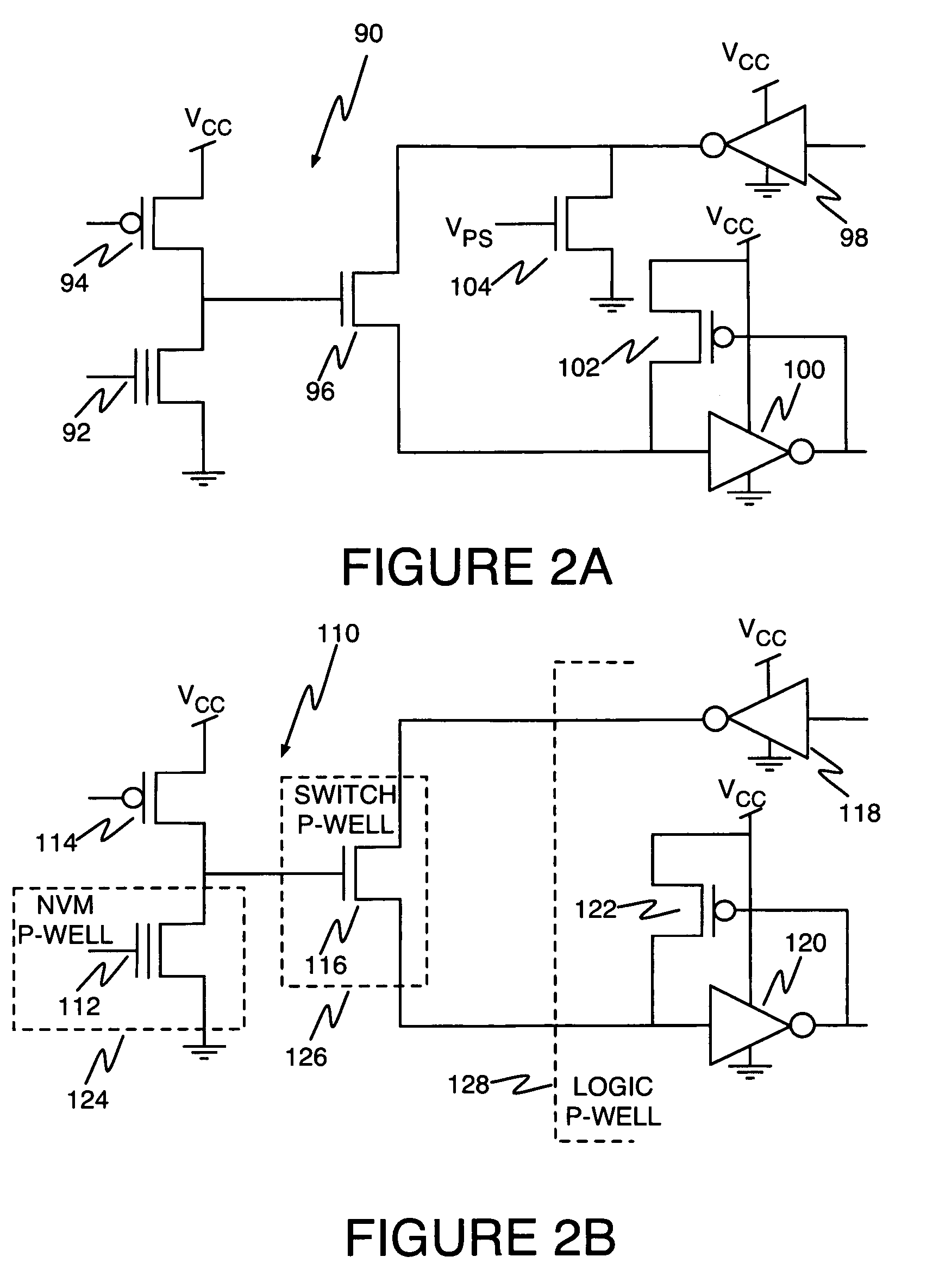
[0016]A non-volatile programmable memory cell suitable for use in a programmable logic array includes a non-volatile MOS transistor in series with a volatile MOS transistor. The non-volatile MOS transistor may be a floating gate transistor, such as a flash transistor, or may be another type of non-volatile transistor such as a floating charge-trapping SONOS, MONOS transistor, or a nano-crystal transistor. A switch that may comprise a volatile MOS transistor, an inverter, or a buffer may be driven by coupling its gate or input to the common connection between the non-volatile MOS transistor and the volatile MOS transistor. The non-volatile MOS transistor and the switch are isolated from one another by forming the non-volatile MOS trans...


PUM


Abstract

A non-volatile programmable memory cell suitable for use in a programmable logic array includes a non-volatile MOS transistor of a first conductivity type in series with a volatile MOS transistor of a second conductivity type. The non-volatile MOS transistor may be a floating gate transistor, such as a flash transistor, or may be another type of non-volatile transistor such as a floating charge-trapping SONOS, MONOS transistor, or a nano-crystal transistor. A volatile MOS transistor, an inverter, or a buffer may be driven by coupling its gate or input to the common connection between the non-volatile MOS transistor and the volatile MOS transistor.

Description

BACKGROUND OF THE INVENTION[0001]1. Field of the Invention[0002]The present invention relates to non-volatile-memory based programmable logic devices. More particularly, the present invention pertains to memory cells for use in non-volatile-memory based programmable logic devices such as field-programmable-gate-array (FPGA) devices.[0003]2. The Prior Art[0004]Numerous non-volatile memory cells have been proposed for use in programmable logic devices such as FPGAs. As non-exhaustive examples, U.S. Pat. No. 6,144,580 discloses embodiments where p-channel and n-channel non-volatile MOS transistors are connected in series and have different control gate connection arrangements. U.S. Pat. No. 6,356,478 discloses p-channel and n-channel non-volatile MOS transistors sharing a common floating gate and a common control gate. U.S. Pat. No. 5,740,106 discloses several different variations on p-channel and n-channel non-volatile MOS transistors connected in series. Some share common floating ga...

Claims


Application Information

Patent Timeline
IPC IPC(8): H01L29/76
CPCG11C16/0433H01L27/11517H01L27/11807H01L27/105H10B41/00
Inventor DHAOUI, FETHIMCCOLLUM, JOHNHAWLEY, FRANKWILKINSON, LESLIE RICHARD
Owner MICROSEMI SOC
Learn More