Probe station with two platens

a technology of probe station and platen, which is applied in the direction of measurement device, semiconductor/solid-state device testing/measurement, instruments, etc., can solve the problems of limited space available insufficient space on the platen to effectively accommodate all the necessary positioners, and limited space for extending the probe through the platen. , to achieve the effect of increasing the difficulty of positioning electrical and optical probes, the limited space is significan

Inactive Publication Date: 2008-05-06
CASCADE MICROTECH
View PDF937 Cites 17 Cited by
  • Summary
  • Abstract
  • Description
  • Claims
  • Application Information

AI Technical Summary

Benefits of technology

[0003]Probe stations are designed to measure the characteristics of electrical devices such as silicon wafers. Probe stations typically include a chuck that supports the electrical device while it is being probed by needles or contacts on a membrane situated above the chuck. In order to provide a controlled environment to probe the electrical device, many of today's probe stations surround the chuck with an environmental enclosure so that temperature, humidity, etc. may be held within predetermined limits during testing. Environmental enclosures protect the device from spurious air currents that would otherwise affect measurements, and also facilitate thermal testing of electrical devices at other-than-ambient environmental conditions. Environmental conditions within the enclosure are principally controlled by a dry air ventilation system as well as a temperature element, usually located below the chuck, that heats or cools the electrical device being tested through thermal conduction.
[0005]Probe stations incorporating EMI shielding structures will usually at least partially surround the test signal with a guard signal that closely approximates the test signal, thus inhibiting electromagnetic current leakage from the test signal path to its immediately surrounding environment. Similarly, EMI shielding structures may provide a shield signal to the environmental enclosure surrounding much of the perimeter of the probe station. The environmental enclosure is typically connected to earth ground, instrumentation ground, or some other desired potential.
[0011]What is desired, then, is a probe station that facilitates accurate alignment of electrical and optical probes.

Problems solved by technology

As it may be observed, when testing devices that include both optical and electrical attributes the number of positioners may be significant thereby potentially resulting in insufficient space on the platen to effectively accommodate all the necessary positioners.
In addition, the opening provided by the platen is normally relatively small so that the space available for extending the probes through the platen is limited.
This limited space significantly increases the difficultly in positioning the electrical and optical probes.
Similarly, the end of the optical probes typically need to be positioned within 0.10 microns in x / y / z directions which is somewhat awkward from a position on the platen above the chuck.
Moreover, the angular orientation of the end portion of the optical probe likewise needs to be very accurate to couple light between the optical probe and the device under test which is similarly difficult.
Moreover, during the testing of wafers the optical probes frequently tend to be out of alignment requiring manual alignment for each photonics device while probing each of the devices.

Method used


Image

  • Probe station with two platens
  • Probe station with two platens
  • Probe station with two platens

Examples


Embodiment Construction

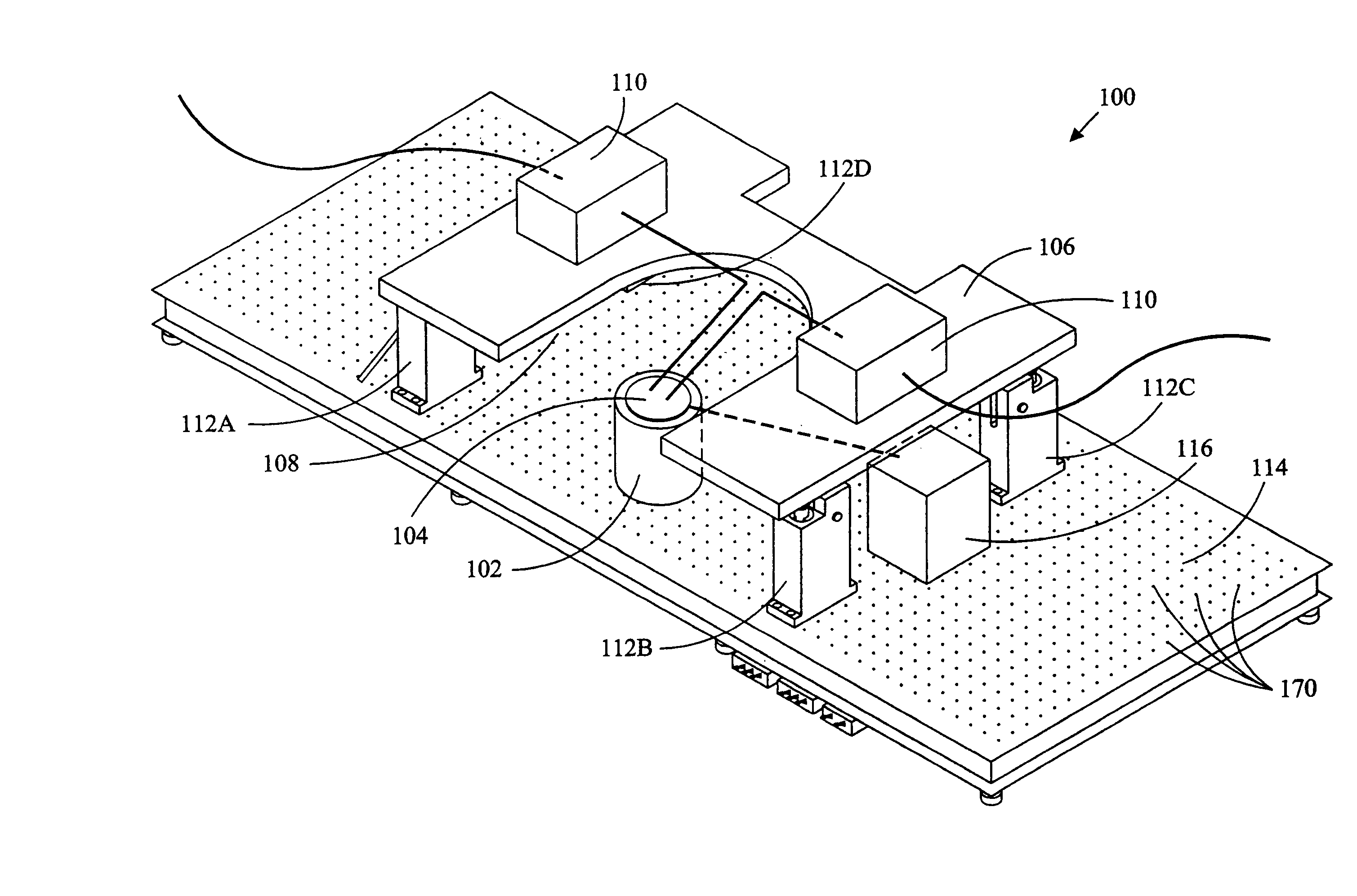
[0023]During testing, the end of the optical probes are typically aligned with the edge of the device under test while the electrical probes are typically aligned with the contacts on the upper surface of the device under test, with both the electrical probes and the optical probes being supported by the platen. In many cases, the entire platen is moved in the z-axis direction for selectively contacting the electrical probes on the device under test. Alternatively, the chuck is moved in a z-axis direction. The z-axis movement of the platen permits consistent simultaneous relative movement of all the electrical and optical probes. Each component of the device under test is successively moved in x and / or y lateral directions relative to the electrical probes using a chuck or other support to a location under the electrical probes.

[0024]The present inventors considered the z-axis movement of the platen or chuck to perform simultaneous probing and came to the realization that normal z-a...


PUM


Abstract

A probe station for testing a device under test. A first platen supporting an electrical probe. A chuck supporting the device under test. A second platen supporting an optical probe. The first platen and the second platen positioned above the device under test. A percentage of the top surface of the second platen terminating into free space.

Description

BACKGROUND OF THE INVENTION[0001]This application is a continuation of U.S. patent application Ser. No. 10 / 285,135 filed Oct. 30, 2002, now U.S. Pat. No. 6,777,964 which claims the benefit of U.S. Provisional Patent Application Ser. No. 60 / 351 ,844 filed Jan. 25, 2002.[0002]The present invention relates to a probe station.[0003]Probe stations are designed to measure the characteristics of electrical devices such as silicon wafers. Probe stations typically include a chuck that supports the electrical device while it is being probed by needles or contacts on a membrane situated above the chuck. In order to provide a controlled environment to probe the electrical device, many of today's probe stations surround the chuck with an environmental enclosure so that temperature, humidity, etc. may be held within predetermined limits during testing. Environmental enclosures protect the device from spurious air currents that would otherwise affect measurements, and also facilitate thermal testi...

Claims


Application Information

Patent Timeline
Patent Type & Authority Patents(United States)
IPC IPC(8): G01R31/02G01R1/18G01R31/28G01R31/311H01L21/66
CPCG01R31/2831G01R31/2886G01R31/2887G01R1/18G01R31/311
Inventor NAVRATIL, PETERFROEMKE, BRADSTEWART, CRAIGLORD, ANTHONYSPENCER, JEFFRUNBAUGH, SCOTTFISHER, GAVINMCCANN, PETEJONES, ROD
Owner CASCADE MICROTECH
Why Eureka
Try Eureka