Phase lock loop indicator

a phase lock loop and indicator technology, applied in the direction of oscillator tubes, pulse automatic control, electrical apparatus, etc., can solve the problems of affecting the locking speed and jitter performance of phase-locked loops. achieve the effect of improving the locking speed and jitter performance of phase-locked loops, and being easy to have a good

Active Publication Date: 2008-05-13
SEMICON MFG INT (SHANGHAI) CORP
View PDF10 Cites 20 Cited by
  • Summary
  • Abstract
  • Description
  • Claims
  • Application Information

AI Technical Summary

Benefits of technology

[0010]The present invention relates to PLLs. One embodiment of the present invention provides a method for realizing the function of lock detection that makes it easier to have a good control on the loop bandwidth. The present embodiment improves the locking speed and jitter performance of phase-locked loops.
[0011]The present embodiment provides one or more of the following advantages: (1) makes it easy to know when the phase-locked loop is locked, (2) makes the phase-locked loop be locked faster, and (3) makes the phase-locked loop be very stable with ultra high jitter performance after it has been locked.
[0012]According to one embodiment, a phase locked loop comprises an input reference clock which is applied to the phase frequency detector and compared with a divided quotient signal which is proportional to the output of the voltage controlled oscillator. The continuous three comparisons of the phase differences are provided to the LOCKDT (FIG. 2, numeral 211). Then LOCKDT indicates the PLL has been locked by outputting an appropriate signal. The output of the LOCKDT is used to control the E DIV (FIG. 2, numeral 209) in bypass or divider mode. This helps to further decrease the input reference frequency, suppress the noise from the input and makes this time the start point when the phase locked loop is switched to a second state with an “ultra” narrow bandwidth.

Problems solved by technology

However, switching activities in digital system will introduce supply and substrate noises which will perturb the sensitive block in PLL.
Any noise injected inside PLL contributes a source of jitter.
These will worsen the jitter performance.

Method used


Image

  • Phase lock loop indicator
  • Phase lock loop indicator
  • Phase lock loop indicator

Examples


Embodiment Construction

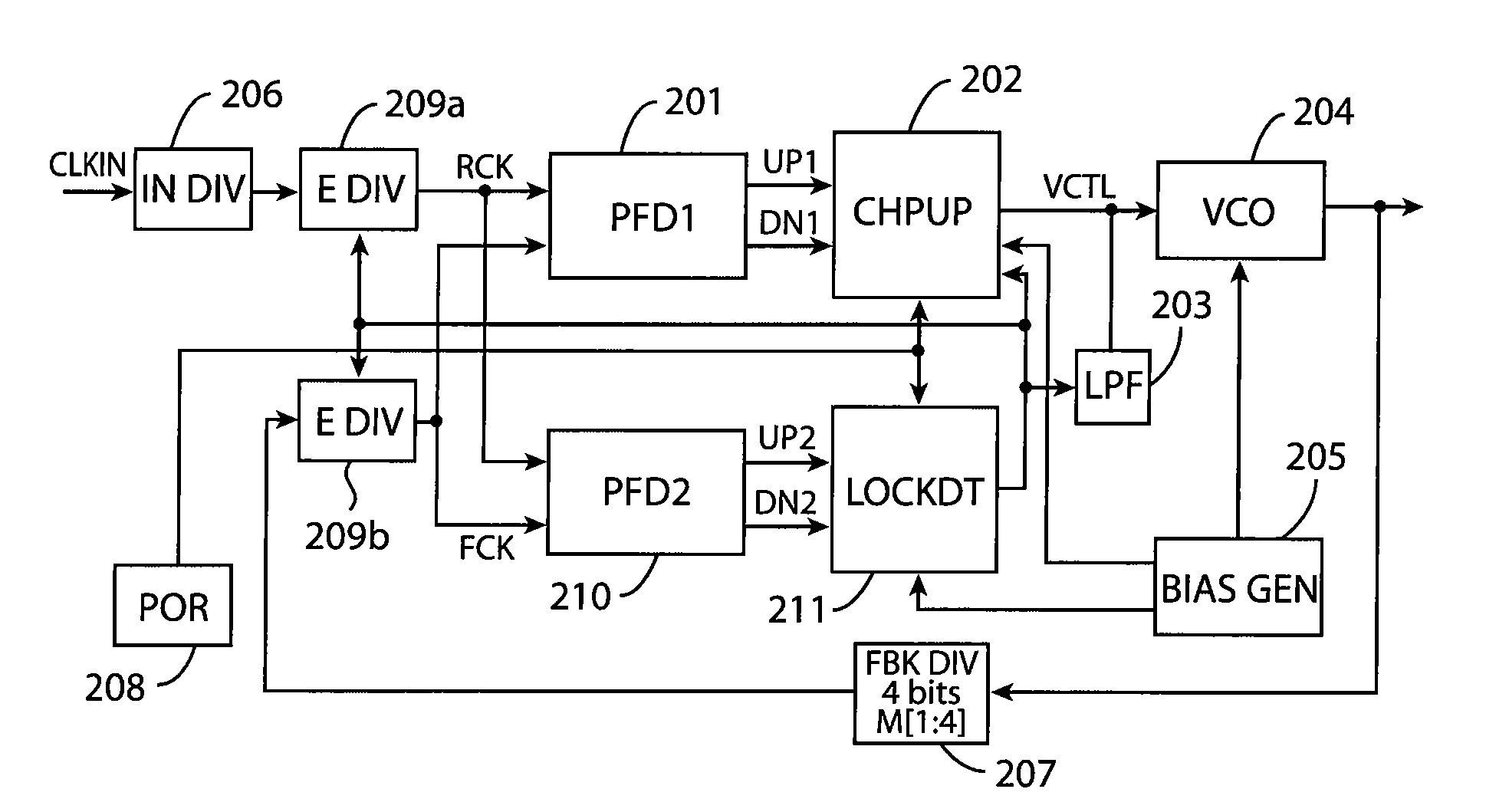
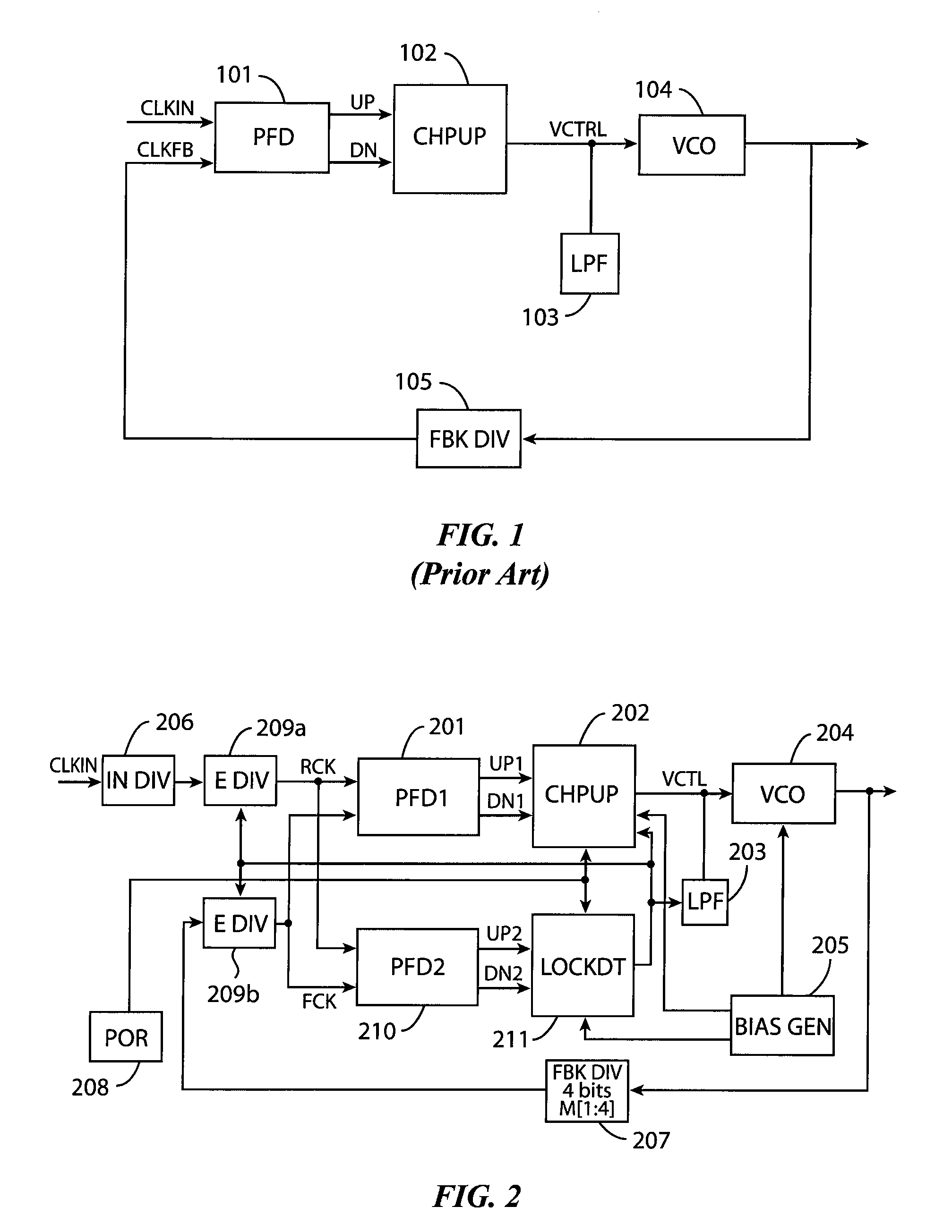
[0025]FIG. 2 is a functional block diagram of one embodiment of the present invention. A phase frequency detector 201, a charge-pump 202, loop filter 203, voltage controlled oscillator (VCO) 204, an input divider 206 and a feedback divider 207 are provided. The input divider provides a reference clock / signal. The first phase frequency detector 201 outputs signals UP1 (or high signal) or DN1 (or low signal) to the charge pump 202, which outputs to VCO 204. A second phase frequency detector 210 that has a different delay than that of the first phase frequency detector 201 is provided. In the present implementation, the second frequency detector has a greater delay than the first frequency detector 201. The delay is used to hold sample data.

[0026]A lock-state detector 211 is also provided to receive outputs signals UP2 (or high signal) and DN 2 (or low signal) from the second phase frequency detector 210. A current generator (or bias generator) 205 provides a reference current for the ...


PUM


Abstract

A phase-locked loop (PLL) circuit includes a power-on-reset (POR) to reset a digital block and set an initial input voltage value VCTRL of voltage-controlled oscillator (VCO). An input divider and a feedback divider are provided to set the frequency ratio of output to input and to raise the resolution of the output frequency. First and second phase frequency detectors are used to measure the phase difference between the two input signals and generate a pulse corresponding to the phase difference. First and second reducing dividers are inserted before the first and second phase frequency detectors to decrease the input frequency of the respective phase frequency detector and keep the ratio of the input frequency and natural frequency (Wn) as a constant. A lock-state detector is used to detect whether the PLL is locked or unlocked. A charge pump is used to provide charge signals corresponding to the pulse. A loop filter is coupled to the output node of the charge pump to provide a voltage VCTRL responding to the charge signals.

Description

CROSS-REFERENCES TO RELATED APPLICATIONS[0001]This application claims priority to Chinese Application No. 200510110860.1; filed on Nov. 29, 2005; commonly assigned, and of which is hereby incorporated by reference for all purposes.BACKGROUND OF THE INVENTION[0002]The present invention relates to the field of integrated circuits technology, more particularly to phase-locked loops. Phase-locked loops (PLLs) are widely used in high performance digital systems. One application it is used is to multiply low frequency clock signals to high frequency clock signals with low jitter. With recent advances in the digital circuit technologies, more stringent performance requirements, including extremely low jitter, have been placed on PLLs. However, switching activities in digital system will introduce supply and substrate noises which will perturb the sensitive block in PLL. Any noise injected inside PLL contributes a source of jitter.[0003]The loop bandwidth can be optimized according to the l...

Claims


Application Information

Patent Timeline
Patent Type & Authority Patents(United States)
IPC IPC(8): H03L7/095H03L7/087
CPCH03L7/087H03L7/0898H03L7/095H03L7/107H03L7/1972H03L2207/04H03L7/1072Y10S331/02
Inventor FU, ZHI GANG
Owner SEMICON MFG INT (SHANGHAI) CORP
Why Eureka
Try Eureka