Structures for coupling and grounding a circuit board in a plasma display device

a plasma display device and circuit board technology, applied in the direction of printed circuit assembling, coupling device connection, gas-filled discharge tube, etc., can solve the problems of poor grounding, loose bolts, damage or distortion of circuit boards, etc., to achieve stable fixation of circuit boards and effective grounding of circuit boards

Inactive Publication Date: 2008-05-27
SAMSUNG SDI CO LTD
View PDF8 Cites 8 Cited by
  • Summary
  • Abstract
  • Description
  • Claims
  • Application Information

AI Technical Summary

Benefits of technology

[0009]The present invention provides a plasma display device having coupling and grounding structures that can effectively ground a circuit board, and stably fix the circuit board to a chassis of the plasma display device.

Problems solved by technology

I have determined that in such a case, the circuit board may be damaged or distorted due to the bolts being over tightened.
Additionally, the bolts may be loosened during thermal distortion or vibration of the circuit board.
Accordingly, the grounding is performed poorly.
Also, if the grounding of the circuit board is performed poorly, current and voltage noises cannot be controlled effectively, and electromagnetic interference (EMI) characteristics will be lowered.

Method used


Image

  • Structures for coupling and grounding a circuit board in a plasma display device
  • Structures for coupling and grounding a circuit board in a plasma display device
  • Structures for coupling and grounding a circuit board in a plasma display device

Examples


Embodiment Construction

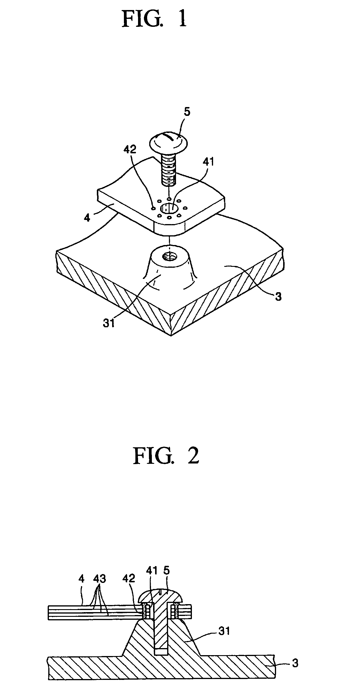
[0029]Shown in FIG. 1 is a plurality of soldering units 42 for grounding formed around a coupling hole 41 for bolt member 5. Circuit board 4 is grounded to a chassis base 3 through a boss 31 as shown in FIGS. 1 and 2.

[0030]The soldering units 42 penetrate circuit board 4 as shown in FIG. 2. In general, the circuit board 4 has a multi-layered structure, and a plurality of circuit ground wires 43 are built-in the cross section of the board. The soldering units 42 penetrate the ground wires 43, and upper end portions of the soldering units 42 are exposed on outer upper side of the circuit board 4.

[0031]As shown in FIG. 2, the head of the coupling bolt member 5 contacts the soldering units 42 to form a ground. That is, the ground wires 43 of the circuit board 4 are grounded to the chassis base 3 through the soldering units 42 and the bolt member 5.

[0032]In the above grounding structure, however, since the soldering units 42 protrude on the upper surface of the circuit board 4, the bolt ...


PUM


Abstract

A coupling and grounding structure of a plasma display device for grounding a circuit board effectively, and fixing the circuit board stably. The plasma display device includes a plasma display panel having a display area, on which images are displayed; a chassis base coupled to a back surface of the plasma display panel; at least one circuit board, on which at least one electronic element for driving the plasma display panel is mounted, the circuit board having a conductive portion and at least one coupling hole to be coupled to the chassis base by a bolt member penetrating the coupling hole; and at least a conductive member which contacts the conductive portion and the bolt member in the coupling hole.

Description

CLAIM OF PRIORITY[0001]This application makes reference to, incorporates the same herein, and claims all benefits accruing under 35 U.S.C §119 from an application entitled PLASMA DISPLAY DEVICE HAVING STRUCTURES FOR COUPLING AND GROUNDING OF CIRCUIT BOARD earlier filed in the Korean Industrial Property Office on 10 Oct. 2003, and there duly assigned Serial No. 2003-70595 by that Office.BACKGROUND OF THE INVENTION[0002]1. Field of the Invention[0003]The present invention relates to a plasma display panel (PDP), and more particularly, to coupling and grounding structures of a circuit board in a plasma display device.[0004]2. Description of the Related Art[0005]In general, a plasma display panel (PDP) displays images using gas discharge operations, and has excellent display characteristics such as display capacitry, brightness, contrast, residual image, and viewing angle. Thus, the PDP can substitute for a cathode ray tube (CRT). In the PDP, a discharge occurs in a gas between electrod...

Claims


Application Information

Patent Timeline
Patent Type & Authority Patents(United States)
IPC IPC(8): H01J17/49H02B1/00H05K5/02H05K7/04G09F9/00H01J17/16H01R4/34H01R4/66H05K3/32
CPCH01R4/66H05K1/0215H05K3/325H01R4/34H05K2201/10295H05K2201/10386H05K2201/10401H05K2201/10409H01J11/10H01J17/16H04N5/645
Inventor KIM, MYOUNG-KON
Owner SAMSUNG SDI CO LTD
Why Eureka
Try Eureka