Semiconductor device

a semiconductor and device technology, applied in the direction of solid-state devices, basic electric elements, electrical apparatus construction details, etc., can solve the problems of disadvantageously deteriorating the electric property of regulatory ic and good thermal radiative properties, and achieve the effects of durable and reliable semiconductor devices, small or narrow planes, and reduced plane occupation areas

Inactive Publication Date: 2008-06-03
SANKEN ELECTRIC CO LTD
View PDF6 Cites 8 Cited by
  • Summary
  • Abstract
  • Description
  • Claims
  • Application Information

AI Technical Summary

Benefits of technology

[0009]The present invention can provide a semiconductor device of smaller or narrowed plane size due to the reduced plane occupation area of semiconducting elements. Also, heat generated from first semiconducting element can be well radiated, and first and second semiconducting elements can be thermally isolated from each other so that operating heat from first semiconducting element never deteriorates electric property of second semiconducting element to provide durable and reliable semiconductor devices.

Problems solved by technology

However, semiconductor device shown in FIG. 8 cannot indicate good thermally radiative property due to the less heat discharging performance because heat emitted from power semiconducting element 21 is discharged to outside only through support plate 3.
In this case, there would be a risk of disadvantageously deteriorating the electric property of regulatory IC 22 which may be overheated by heat directly transferred to regulatory IC 22 from power semiconducting element 21.
The apposed structure of FIG. 9 also has an additional disadvantage because it requires larger plane size of semiconductor device in the apposed structure of power semiconducting element 21 and regulatory IC 22 on support plate 3.

Method used


Image

  • Semiconductor device
  • Semiconductor device
  • Semiconductor device

Examples


Embodiment Construction

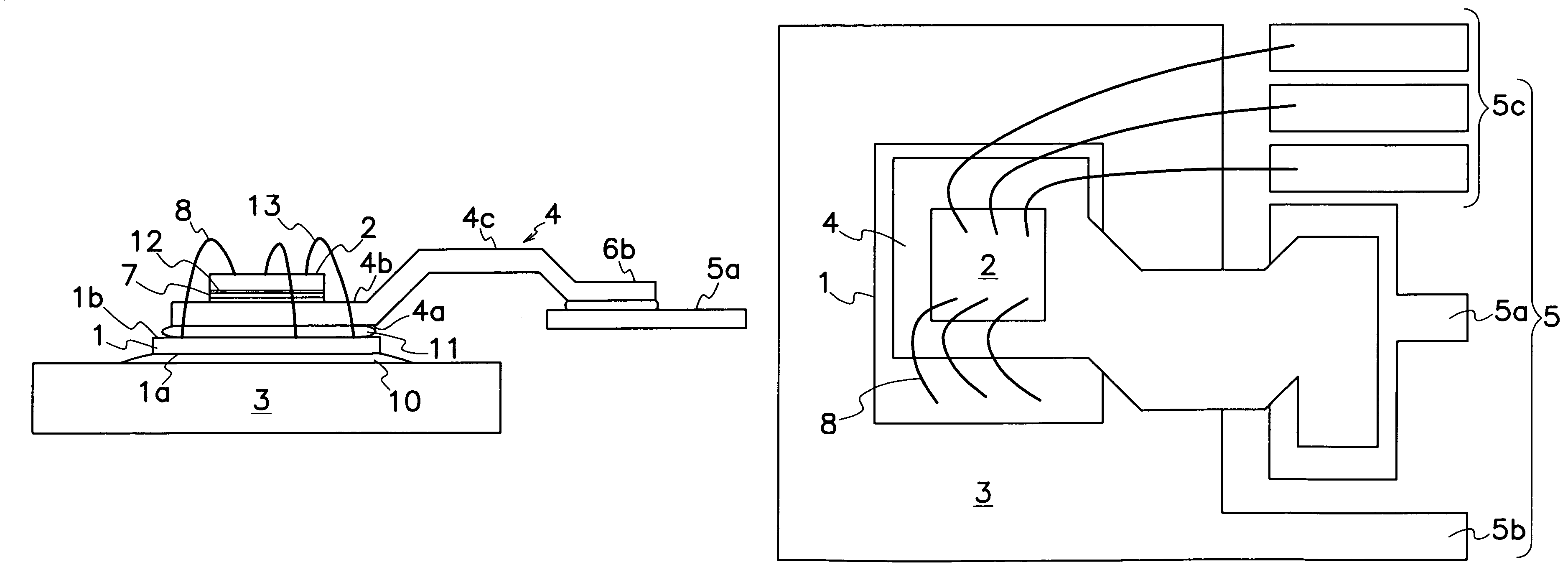
[0021]Embodiments will be described hereinafter in connection with FIGS. 1 to 7 of the drawings regarding the semiconductor device according to the present invention applied to a power semiconductor device for use in a switching regulator.

[0022]As shown in FIG. 1, the semiconductor device according to the present invention comprises a MOS-FET 1 as a first semiconducting element or switching element whose one main surface 1a is mounted or secured on a support plate 3 through an electrically conductive adhesive or solder 10. Formed of nickel-plated, thermally radiative and electrically conductive metal such as copper or aluminum is support plate 3 to which one main electrode of MOS-FET 1 is electrically connected. The other main electrode, namely source electrode is formed on the other main surface 1b of MOS-FET 1 on the opposite side of support plate 3, and a connecting lead 4 is attached on source electrode of MOS-FET 1 via electrically conductive adhesive or solder 11.

[0023]As show...


PUM


Abstract

A semiconductor device is provided which comprises a connecting lead 4 mounted between a MOS-FET 1 and a regulatory IC 2 on a support plate 3. Connecting lead 4 has a thermally radiative and electrically conductive substrate 6 and electrically insulative and thermal transfer-resistive covering 7. Substrate 6 has one end 6a providing one main surface 4a of connecting lead 4 which is mounted and electrically connected on the other main surface 1b of MOS-FET 1. Covering 7 provides the other main surface 4b of connecting lead 4 for supporting regulatory IC 2 at one end 6a of substrate 6. When electric current flow is supplied to MOS-FET 1 through an electrified path of support plate 3 and substrate of connecting lead 4, heat produced from operating MOS-FET 4 is effectively radiated through support plate 3 and substrate 6 of connecting lead 4 to improve thermal radiation in the semiconductor device in the layered structure of the semiconducting elements while heavy current can flow through MOS-FET 1 due to sufficient heat radiation.

Description

TECHNICAL FIELD[0001]This invention relates to a semiconductor device, in particular, of the type which has semiconducting elements on their reduced plane occupation area so that the semiconductor device has the excellent thermally radiative property even in its narrowed plane size.BACKGROUND OF THE INVENTION[0002]A semiconductor device is known which has an integral package of a power semiconducting element and a regulatory IC for controlling the power semiconducting element. As shown in FIG. 8, the semiconductor device of this type comprises a support plate 3; a power semiconducting element 21 mounted on support plate 3; a layered structure of a regulatory IC 22 mounted on power semiconducting element 21 or, as shown in FIG. 9, an apposed structure of a regulatory IC 22 secured on support plate 3 away from power semiconducting element 21. For example, FIG. 4 of Japanese Patent No. 2,566,207 discloses a semiconductor device of such a layered structure.[0003]Such a semiconductor dev...

Claims


Application Information

Patent Timeline
Patent Type & Authority Patents(United States)
IPC IPC(8): H01L31/111H05K7/20H01L23/34H01L21/822H01L23/36H01L23/495H01L25/065H01L25/07H01L25/16H01L25/18H01L27/00H01L27/04
CPCH01L23/36H01L23/49562H01L23/49575H01L24/49H01L2924/1306H01L2924/014H01L24/48H01L2924/14H01L2924/13091H01L2924/01082H01L2924/01033H01L2924/01029H01L2924/01028H01L2924/01014H01L2224/32245H01L2224/48091H01L2224/48137H01L2224/48247H01L2224/49H01L2224/73265H01L2924/01004H01L2924/01005H01L2924/01006H01L2924/01013H01L2924/00014H01L2924/00H01L2924/181H01L2224/45099H01L2224/05599
Inventor TERAO, KOHTARO
Owner SANKEN ELECTRIC CO LTD
Why Eureka
Try Eureka