Nonvolatile memory cell and methods for operating a nonvolatile memory cell

Inactive Publication Date: 2008-06-10
POLARIS INNOVATIONS LTD
View PDF18 Cites 3 Cited by
  • Summary
  • Abstract
  • Description
  • Claims
  • Application Information

AI Technical Summary

Benefits of technology

[0011]According to embodiments of the invention, the nonvolatile memory cell has a programmable component, the electrical resistance of which depends on its programming state. In particular, the programmable component has two different programming states that are interpreted as logic “1” and logic “0”. The nonvolatile memory cell can furthermore have at least one first switching element, which is connected to a first word line, and also at least one second switching element, which is connected to a second word line. The first switching element has the effect that when the first word line is activated, a first current path leading from one of the two bit lines via the programmable component as far as a first potential terminal is switched in conducting fashion. Consequently, when the first word line is activated, the first switching element enables an electrical connection between the respective bit line and a first potential terminal, via which electrical connection a current can flow whose current intensity depends on the magnitude of the electrical resistance of the programmable component. As a result, depending on the programming state of the component, it is possible to effect a change in the potential of that bit line that is connected to the first potential terminal via the first current path.
[0013]According to embodiments of the invention, the “activation” of a word line is to be understood to mean that the corresponding word line is biased such that switching elements connected to the respective word line, such as MOSFETs (metal oxide semiconductor field effect transistor), for example, are switched into the on state, thereby enabling the respective current path. The activation of one word line or the other thus simultaneously brings about the activation of one current path or the other, in which case the fact of whether and with what magnitude a current flows along the respective current path depends on the programming state of the component and the electrical resistance of the component that prevails in this state. Independently of the magnitude of the electrical resistance of the component, however, the activation of the respective word line has the effect that the corresponding current path is activated via the respective switching element.
[0023]It is preferably provided that the second current path contains a protective resistor, which prevents a programming of the programmable component via the second current path. Since both current paths lead via the programmable component, but the second current path additionally contains a protective resistor, the current flowing through the component is lower in the case of the second current path than in the first current path (provided that in each case the same potential difference is applied to the opposite ends of the respective current path). In the case of the second current path, the additional protective resistor keeps the current flowing through the component so low that the current intensity required for reprogramming is not exceeded. In particular, in this embodiment, the memory cell can be operated with two word lines that are driven by in each case identical word line parameters, in particular identical word line potentials. If need be, the control timing during the operation of the first and second word lines may be chosen differently, if appropriate, in order to enable a different type of access to the nonvolatile memory cell than in the case of volatile memory cells.
[0046]It is preferably provided that both current paths are coupled to the first bit line by the respective switching elements, and through the first current path the potential of the first bit line is increased at least when the programmable component is programmed in a low-impedance state, and through the second current path the potential of the first bit line is reduced (or vice versa).
[0048]It is preferably provided that the second time duration is chosen to be greater than the first time duration. By way of example, in order to read from the memory cell, firstly the first word line is activated momentarily and then the second word line is activated over a longer period of time, but only after the first word line has already been deactivated again. The only momentary activation of the first word line prevents unintentional reprogramming of the component.

Problems solved by technology

Even during operation, stored items of information continually have to be refreshed again since they are otherwise lost through leakage currents despite the operating voltage being maintained.

Method used


Image

  • Nonvolatile memory cell and methods for operating a nonvolatile memory cell
  • Nonvolatile memory cell and methods for operating a nonvolatile memory cell
  • Nonvolatile memory cell and methods for operating a nonvolatile memory cell

Examples


Embodiment Construction

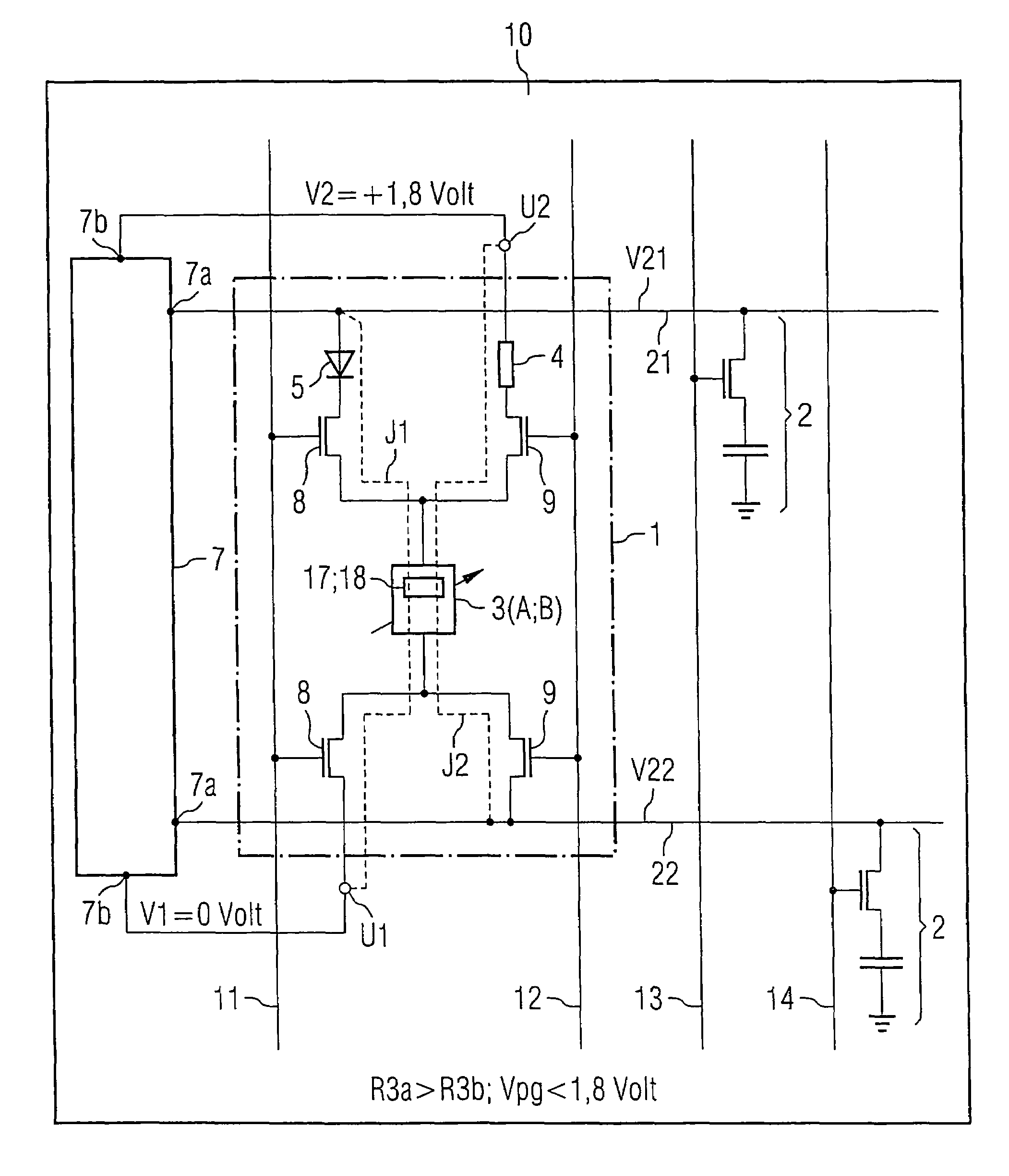
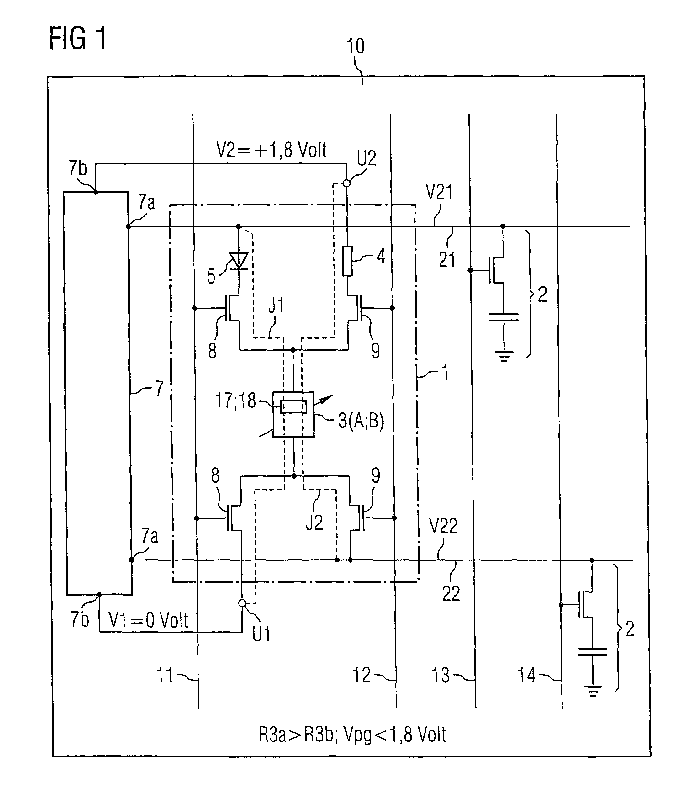
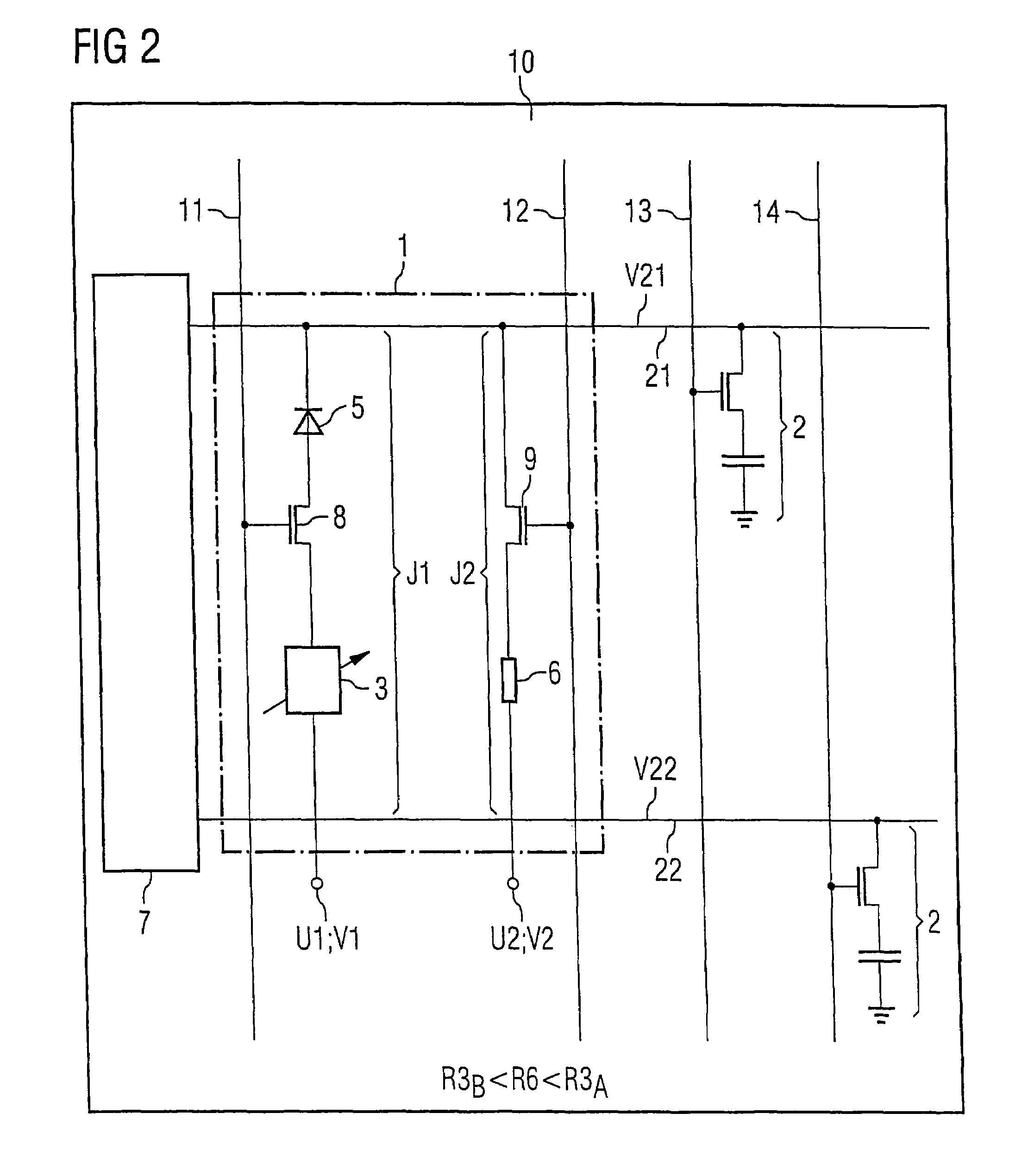
[0061]FIG. 1 shows an integrated semiconductor memory 10, into which is integrated a memory cell 1 according to the invention in accordance with a first embodiment. The memory cell 1 is connected to two word lines 11, 12 and also to two bit lines 21, 22. Volatile memory cells 2 each having a selection transistor and a storage capacitor are furthermore connected to the bit lines 21, 22. The memory cells 2 are connected to further word lines 13, 14. The word lines 11, 12 to which the nonvolatile memory cell 1 according to the invention is connected are formed in the same way as the further word lines 13, 14. In particular, they are operated with the same potentials. As a result, the memory cell according to the invention can be integrated into a memory cell array with volatile memory cells 2 with minimal additional outlay.

[0062]The memory cell 1 has a programmable component 3, which, depending on the programming state, is either at high impedance (programming state A) or at low impeda...


PUM


Abstract

A nonvolatile memory cell (1) can be integrated in space-saving fashion into a semiconductor circuit (10) intended for volatile storage with the aid of volatile memory cells (2). The memory cell (1) has a programmable component (3) having an electrical resistance that can be altered by reprogramming, and also first (8) and second switching elements (9), which switch a first current path (J1) or a second current path (J2) in conducting fashion upon activation of optionally a first (11) or a second word line (12). At least one of the two current paths leads via the programmable component (3). Potentials of two bit lines (21, 22) to which the memory cell (1) according to the invention is connected can be altered as a result of the first or the second current path (J1, J2) being activated temporarily. The memory cell (1) permanently stores an item of digital information and can be driven by word lines (11, 12) and bit lines (21, 22) such as are conventionally used in volatile semiconductor memories (10). The invention opens up the possibility of integrating volatile and nonvolatile memory cells into a common memory cell array.

Description

[0001]This application claims priority to German Patent Application 10 2004 047 638.1, which was filed Sep. 30, 2004, and is incorporated herein by reference.TECHNICAL FIELD[0002]The invention relates to a nonvolatile memory cell and method for operating a non-volatile memory cell.BACKGROUND[0003]In the case of integrated semiconductor memories, a distinction is made between volatile semiconductor memories and nonvolatile semiconductor memories. Nonvolatile semiconductor memories store the items of information even after the operating voltage has been switched off. Nonvolatile semiconductor memories may be EEPROMs (electrically erasable programmable read only memories), for example. By contrast, volatile semiconductor memories store the items of information only during their operation until the operating voltage is switched off. Even during operation, stored items of information continually have to be refreshed again since they are otherwise lost through leakage currents despite the...

Claims


Application Information

Patent Timeline
Patent Type & Authority Patents(United States)
IPC IPC(8): G11C11/00
CPCG11C11/005
Inventor PERNER, MARTIN
Owner POLARIS INNOVATIONS LTD
Why Eureka
Try Eureka