Semiconductor-manufacturing apparatus

a manufacturing apparatus and semiconductor technology, applied in the direction of hot plate heating arrangements, vacuum evaporation coatings, coatings, etc., can solve the problems of difficult to obtain temperature uniformity, complex heating adjusting methods, and inability to achieve sufficiently high temperature uniformity

Active Publication Date: 2008-07-01
APPLIED MATERIALS INC
View PDF9 Cites 28 Cited by
  • Summary
  • Abstract
  • Description
  • Claims
  • Application Information

AI Technical Summary

Benefits of technology

[0011]According to the semiconductor manufacturing apparatus described above, in the susceptor for holding a substrate (target substrate) as a processing target such as a semiconductor wafer or glass substrate, the substrate is held by forming a gap between the target substrate and the substrate heating surface. This decreases influences on the temperature distribution of the substrate such as the local three-dimensional structure on the substrate heating surface and the nonuniformity of the temperature distribution.
[0012]Furthermore, regarding nonuniformities of the temperature and film thickness distributions caused by various types of factors such as a differ

Problems solved by technology

With the method of adjusting the heating condition for the susceptor in accordance with the light irradiating condition and the like, however, when a sufficiently high planar temperature uniformity of the wafer is to be obtained, the heating adjusting method becomes complicated.
Alternatively, due to limi

Method used


Image

  • Semiconductor-manufacturing apparatus
  • Semiconductor-manufacturing apparatus
  • Semiconductor-manufacturing apparatus

Examples


Embodiment Construction

[0020]A preferred embodiment of a semiconductor manufacturing apparatus according to the present invention will be described in detail with reference to the accompanying drawings. In the description of the drawings, the same elements are denoted by the same reference numerals, and a repetitive explanation thereof is omitted. The dimensional proportion of the drawings does not necessarily correspond to that of the described embodiment.

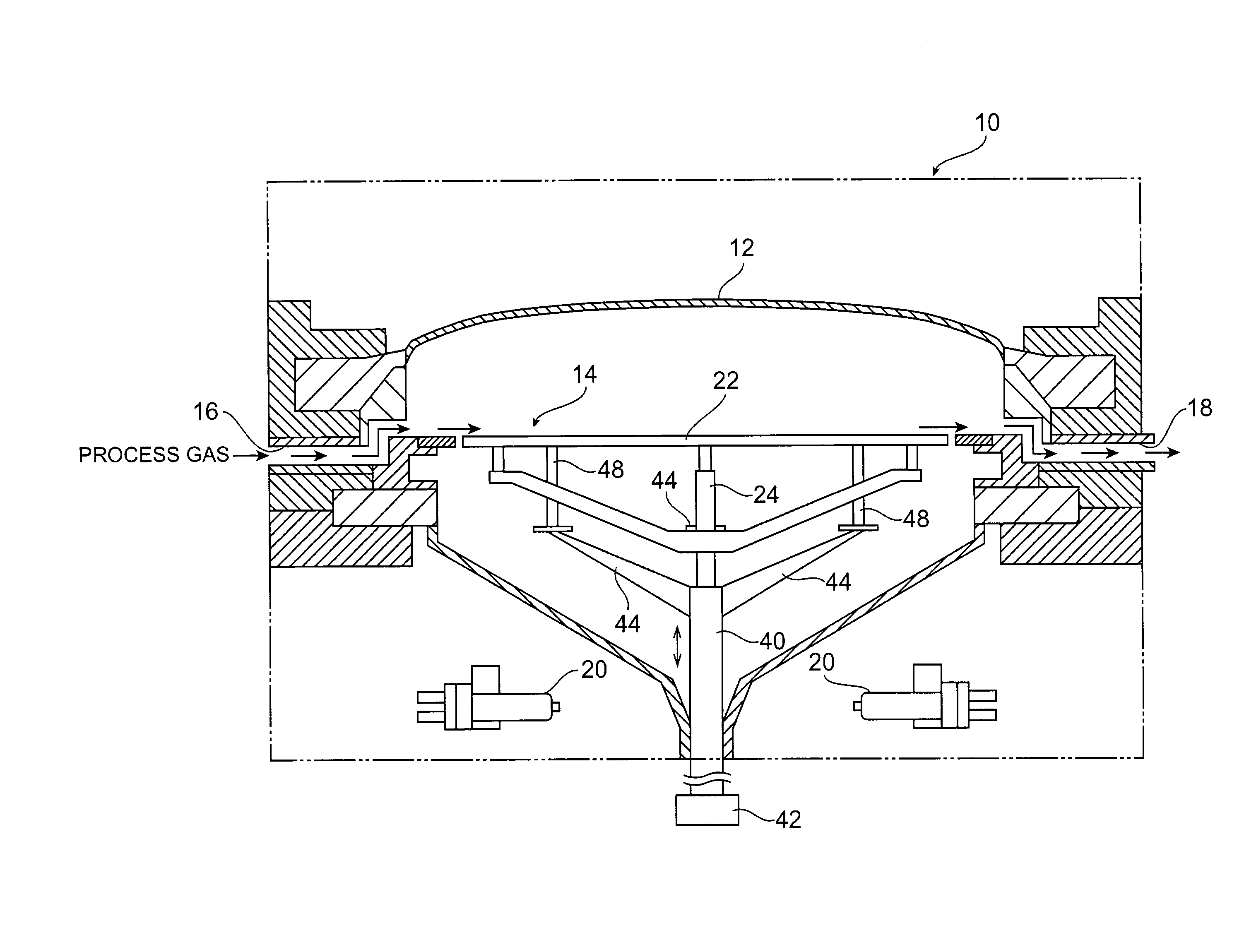
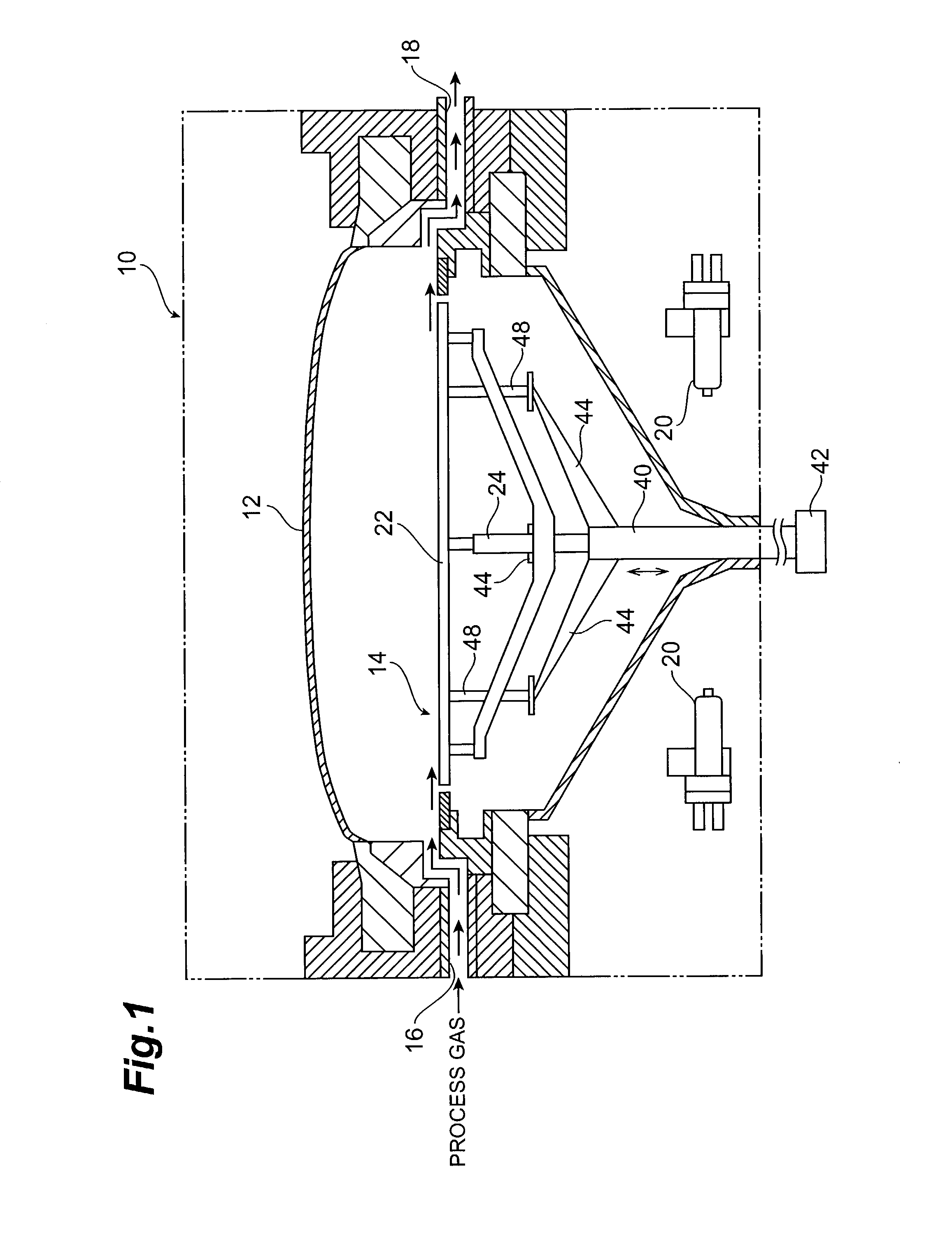
[0021]FIG. 1 schematically shows a film deposition apparatus such as an epitaxial growth apparatus as a semiconductor manufacturing apparatus according to the present invention. A film deposition apparatus 10 shown in FIG. 1 is a single wafer processing type apparatus for processing silicon wafers (not shown in FIG. 1) as target substrates one by one. An example of the target substrate includes a semiconductor wafer and glass substrate. A case wherein the target substrate is a silicon wafer will be described hereinafter.

[0022]The film deposition apparat...


PUM

PropertyMeasurementUnit
Distanceaaaaaaaaaa
Areaaaaaaaaaaa
Distanceaaaaaaaaaa

Abstract

On a wafer holding area 50 on the upper surface of a susceptor 22, a wafer W is supported by a wafer support 54 such that a gap with a predetermined distance is formed between the wafer W and a wafer heating surface 52. A projection 58 that decreases the distance of the gap with respect to the wafer W is formed on the wafer heating surface 52. At this time, the heating condition for the wafer W by the susceptor 22 is adjusted by means of the distances of the gaps at the respective portions of the wafer holding area 50. Thus, the uniformity of the planar temperature distribution of the wafer W and that of the thickness distribution of the formed film can be improved.

Description

TECHNICAL FIELD[0001]The present invention relates to a semiconductor manufacturing apparatus with a susceptor for holding and heating a semiconductor wafer (substrate).BACKGROUND ART[0002]Semiconductor manufacturing apparatuses include one called a single wafer processing type semiconductor manufacturing apparatus for processing silicon wafers one by one. In this single wafer processing type semiconductor manufacturing apparatus, a wafer support unit for horizontally supporting only one wafer is usually arranged in a process chamber.[0003]The wafer support unit generally has a susceptor (substrate holding table) where a wafer is placed. The susceptor is heated by a heating means such as a lamp, and the wafer is heated through the susceptor.[0004]The wafer support unit also has a lift mechanism for vertically moving the wafer placed on the susceptor with respect to the susceptor. The lift mechanism has a plurality of lift pins extending through the susceptor. When the wafer is place...

Claims


Application Information

Patent Timeline
IPC IPC(8): H01L21/00C23C14/00C23C16/00H01L21/205C23C16/458C23C16/46C23C16/52H01L21/26H01L21/68H01L21/687
CPCC23C16/4583C23C16/46H01L21/68735H01L21/6835H01L21/67115H01L21/205
Inventor MAEDA, YUJINAKANISHI, KOJITOKAI, NOBUOKAWAI, ICHIRO
Owner APPLIED MATERIALS INC
Why Eureka
Try Eureka