Substrate processing method

a processing method and substrate technology, applied in semiconductor/solid-state device testing/measurement, liquid/solution decomposition chemical coating, instruments, etc., can solve the problems of inability to perform direct measurement, inability to achieve cost and time, and inability to achieve direct measurement. , to achieve the effect of preventing the variation in quality between substrates and preventing the variation of substrate quality

Active Publication Date: 2008-08-05
EBARA CORP
View PDF30 Cites 3 Cited by
  • Summary
  • Abstract
  • Description
  • Claims
  • Application Information

AI Technical Summary

Benefits of technology

[0012]The present invention has been made in view of the above situation in the related art. It is therefore an object of the present invention to provide a substrate processing method and apparatus which can measure and monitor a thickness and / or properties of a film formed on a substrate as needed, and quickly correct a deviation in process conditions, and which can therefore stably provide a product of constant quality.
[0014]According to the substrate processing method, a film thickness and / or film property of a processed film is measured during and / or after processing, and a film thickness and / or film property is controlled. Thus, the method enables direct measurement and control on a device substrate. This ensures quality of the film even when the film thickness or property has changed with time after continued film processing, and makes it possible to provide a stable product.
[0017]In a preferred embodiment of the present invention, measurement of a change in the film thickness and / or the film property of the metal portion is performed on a particular measurement area by using an optical sensor which is orientable to any point on the substrate. By setting a particular area at the same position on each substrate as a control target, variations in quality between substrates can be prevented.
[0018]In a preferred embodiment of the present invention, measurement of a change in the film thickness and / or the film property of the metal portion is performed on a plurality of measurement areas simultaneously or sequentially by using an optical sensor which is orientable to any point on the substrate. By setting a plurality of areas on a substrate as control targets, variations in quality in the substrate can be prevented.
[0019]The optical sensor may be one which utilizes spectroreflectometry, ellipsometry or spectroscopic ellipsometry. With such an optical sensor, measurement can be performed in a non-destructive manner, i.e. without destroying a substrate, and in a short time of about several seconds to several tens of seconds for one measurement area. This is desirable in light of quality control.
[0022]Take film formation on exposed surfaces of interconnects for example. When selectively covering the exposed surfaces of interconnects with a coating film (protective film), device performance is generally governed primarily by a coating film (protective film) formed on the interconnects. Accordingly, it is most important to control properties of the coating film formed on the interconnects. It is, however, difficult to directly measure a film thickness of the coating film on the interconnects, because the interconnects generally have a width of not more than 1 μm. Even with a continuous coating film having a relatively wide area, film properties may vary at various portions depending upon sizes. According to the above substrate processing method, therefore, a measurement area in which measurement of the film thickness of e.g. a coating film is possible and a target area as a control target are set on a substrate, the film thickness of the coating film formed in the measurement area is measured, and this measured value is converted to the film thickness of the coating film in the target area by using a prepared calibration curve showing a relationship between the film thickness of the coating film in the measurement area and the film thickness of the coating film in the target area. This makes it possible to indirectly determine the film thickness of a coating film, whose measurement is generally impossible, formed on interconnects.

Problems solved by technology

For the above-described discontinuous film selectively covering interconnects or to be cut, however, measurement of the film with a conventional sensor is difficult, and it is required to quickly measure the thickness or properties of such a film in a non-destructive manner.
This method, however, is not practicable in view of cost and time involved.
It is, however, not generally practiced to perform a direct measurement on a substrate formed device as a processing object for adjustment of the process conditions, and the like.
Wet processings, such as plating, etching and electrolytic polishing, often use a liquid chemical comprising a number of chemical components, and it is difficult to monitor and control with accuracy all the components in the liquid chemical.

Method used


Image

  • Substrate processing method
  • Substrate processing method
  • Substrate processing method

Examples


Embodiment Construction

[0057]Preferred embodiments of the present invention will now be described in detail with reference to the drawings.

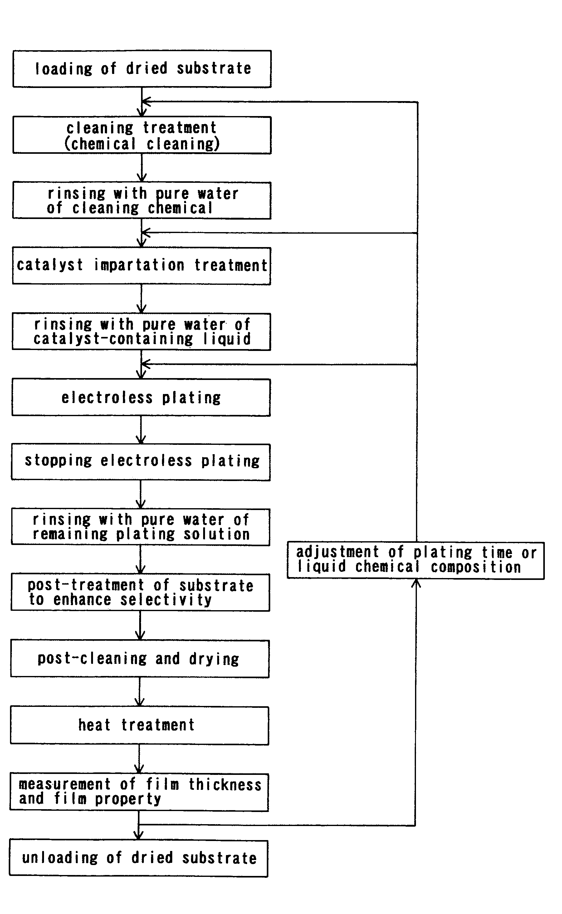
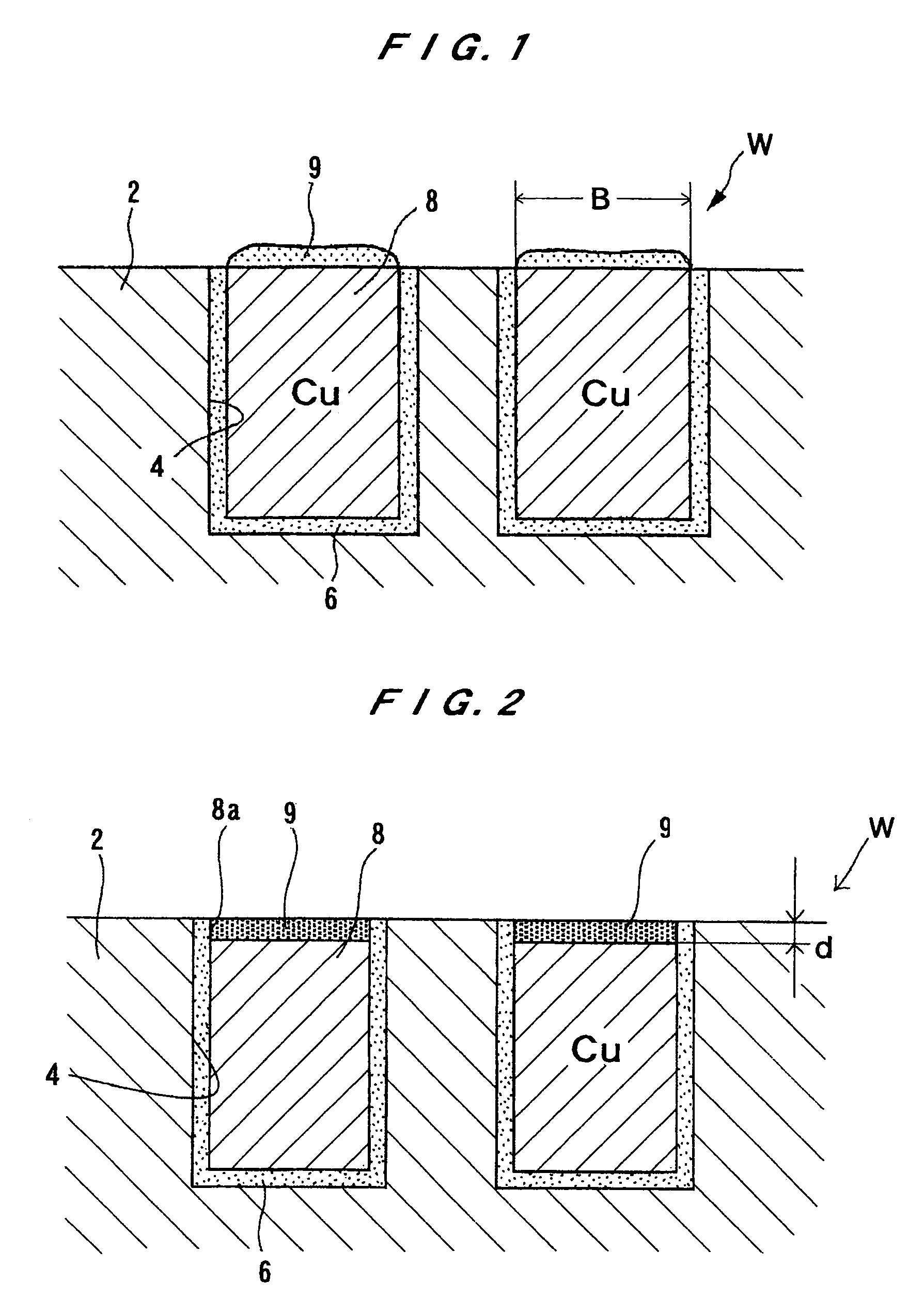
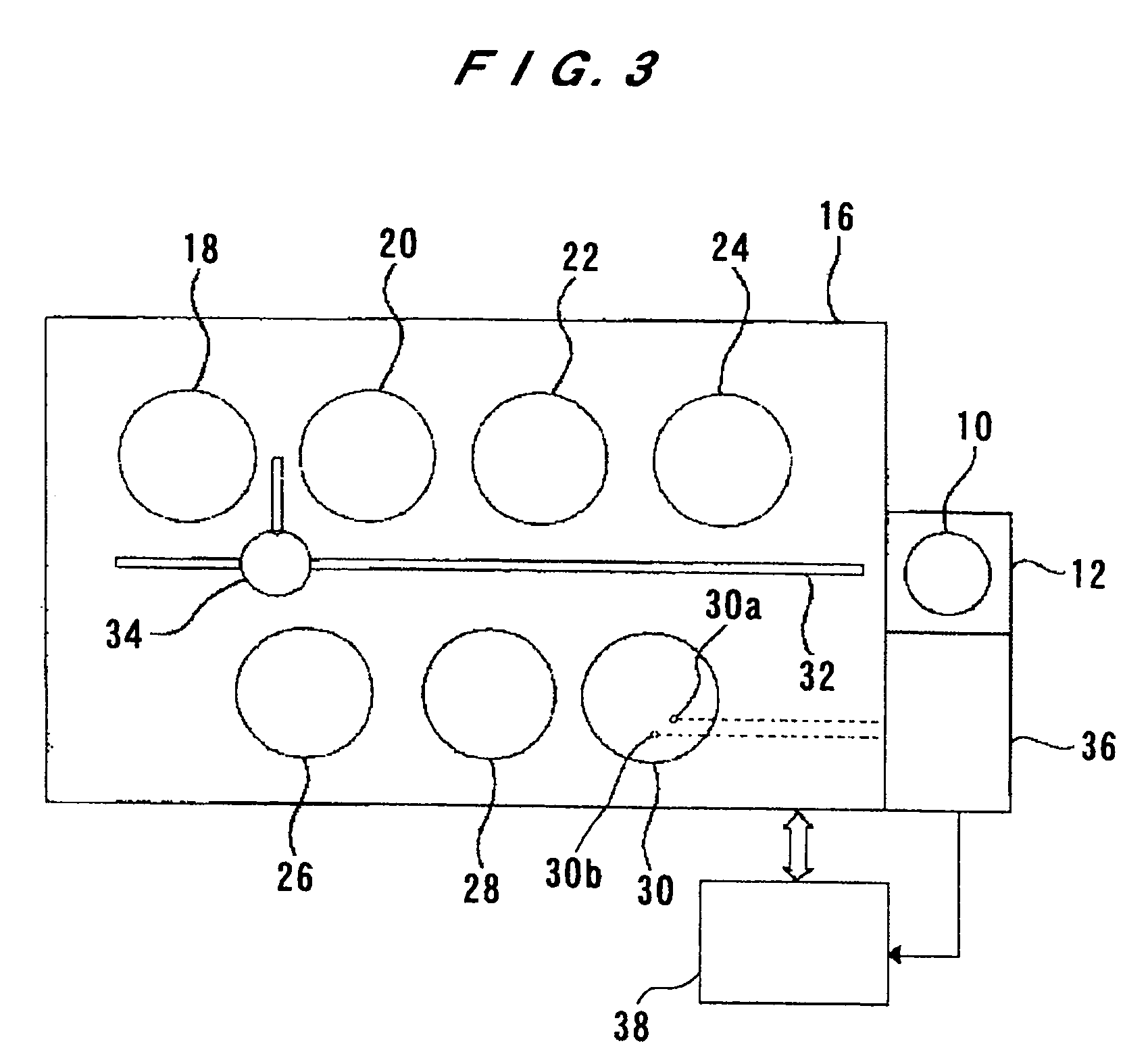
[0058]FIG. 3 shows a layout plan of a substrate processing apparatus according to an embodiment of the present invention. As shown in FIG. 3, the substrate processing apparatus includes a loading / unloading unit 12 housing a substrate cassette 10 that houses substrates W each having interconnects 8 of e.g. copper formed in interconnect recesses 4 which are formed in a surface (see FIG. 1). Along one long side of a rectangular housing 16 provided with a ventilation system, there are disposed in series a first pre-treatment unit 18 for performing cleaning of the surface of a substrate W as a pre-plating treatment, a second pre-treatment unit 20 for imparting a catalyst to exposed surfaces of interconnects 8 after cleaning to activate surfaces of interconnects, an electroless plating unit 22 for performing electroless plating of the surface (processing surface) of the subs...


PUM

PropertyMeasurementUnit
widthaaaaaaaaaa
pHaaaaaaaaaa
temperatureaaaaaaaaaa

Abstract

There is provided a substrate processing method and apparatus which can measure and monitor thickness and / or properties of a film formed on a substrate as needed, and quickly correct a deviation in process conditions, and which can therefore stably provide a product of constant quality. A substrate processing method for processing a substrate having a metal and an insulating material exposed on its surface in such a manner that a film thickness of the metal, with an exposed surface of the metal as a reference plane, is selectively or preferentially changed, including measuring a change in the film thickness and / or a film property of the metal during and / or immediately after processing, and monitoring processing and adjusting processing conditions based on results of this measurement.

Description

BACKGROUND OF THE INVENTION[0001]1. Field of the Invention[0002]This invention relates to a substrate processing method and apparatus, and more particularly to a substrate processing method and apparatus for protecting interconnects by selectively covering exposed surfaces of embedded interconnects, which have been formed by embedding an electric conductor such as copper in a surface of a substrate such as a semiconductor wafer, with a coating film (protective film) of a metal or an alloy.[0003]The present invention also relates to a substrate processing method and apparatus for caving in exposed surfaces of embedded interconnects to form recesses, preparatory to selectively covering exposed surfaces of the embedded interconnects, which have been formed by embedding an electric conductor such as copper in a surface of a substrate such as a semiconductor wafer, with a coating film (protective film) of a metal or an alloy.[0004]2. Description of the Related Art[0005]As a process for f...

Claims


Application Information

Patent Timeline
Patent Type & Authority Patents(United States)
IPC IPC(8): H01L21/66G01B21/08C23C18/16C23C18/31C23F1/08H01L21/288H01L21/3205H01L21/768
CPCH01L21/288H01L21/76849H01L21/76864H01L21/76874H01L22/12C23C18/1879C23C18/1675C23C18/1608H01L22/20C23C18/1692H01L2223/54466
Inventor WANG, XINMINGTAKAGI, DAISUKETASHIRO, AKIHIKOFUKUNAGA, AKIRA
Owner EBARA CORP
Why Eureka
Try Eureka