Debuggable opaque IP

a technology of opaque ip and opaque ip, which is applied in the direction of cad circuit design, program control, instruments, etc., can solve the problems of affecting the system design and debugging process, affecting the design, and leaving the user wondering

Active Publication Date: 2008-08-05
TAHOE RES LTD
View PDF1 Cites 55 Cited by
  • Summary
  • Abstract
  • Description
  • Claims
  • Application Information

AI Technical Summary

Benefits of technology

[0018]In an EDA system, the present invention can be used to allow system designers to view nodes selected and enabled by the IP designer in encrypted or otherwise opaque IP. The parti

Problems solved by technology

Since the IP is essentially opaque to the user, it is not practicable for the user to probe internal nodes (for example, key registers, signals and state machines) to see the IP's state during the system debugging process carried out in simulation and/or running in hardware.
This lack of visibility into an IP core can impede the system design and debugging process and can leave the user wondering if a problem is due to errors in the portion of the system the user designed or a problem with the IP.
Therefore, debugging done inside the hardware using these types of techniques actually leads to changes the design, which is not always desirable.
However, the use of an external logic analyzer to monitor pins of a hardware device has certain limitatio

Method used


Image

  • Debuggable opaque IP
  • Debuggable opaque IP
  • Debuggable opaque IP

Examples


Embodiment Construction

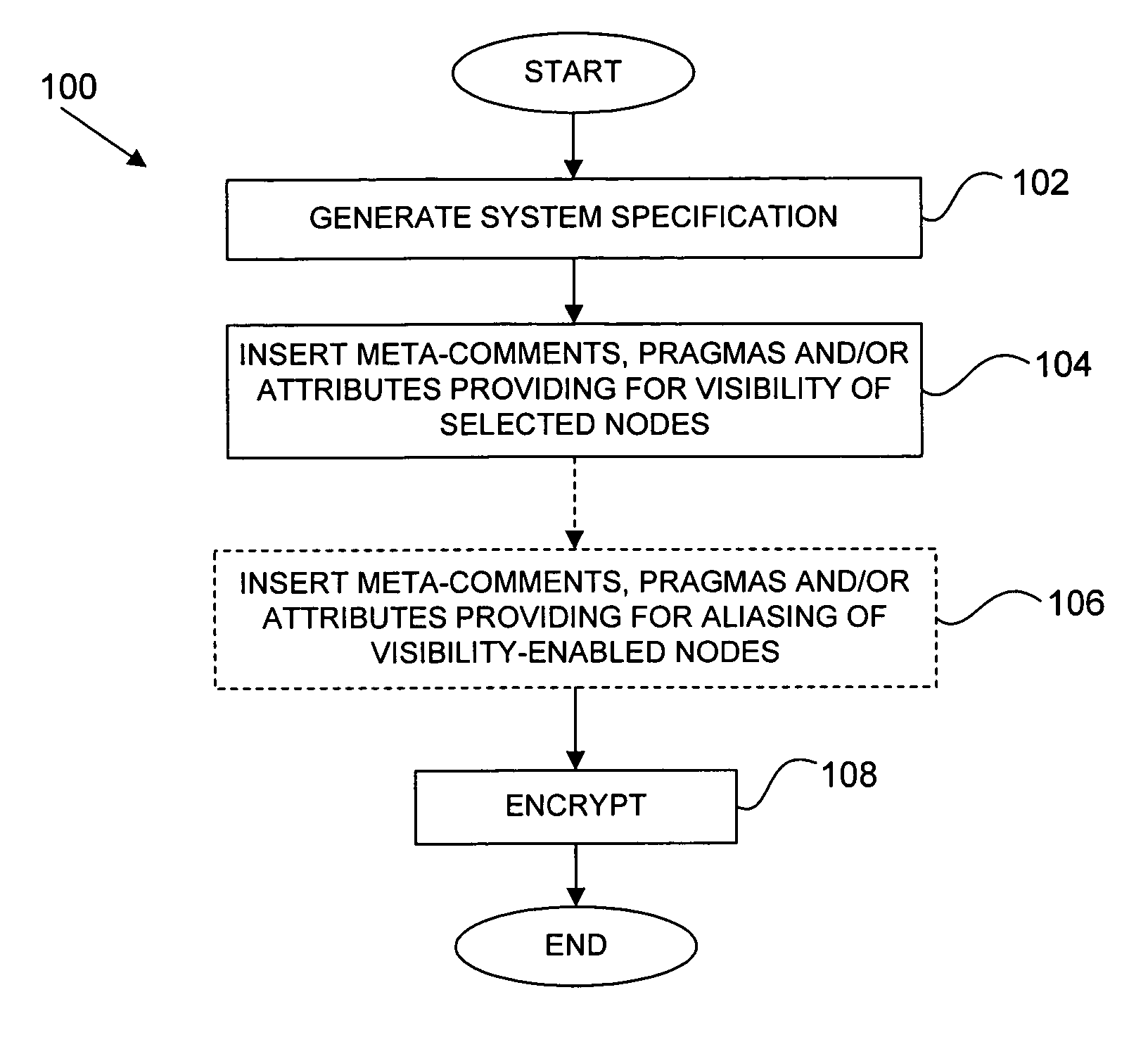
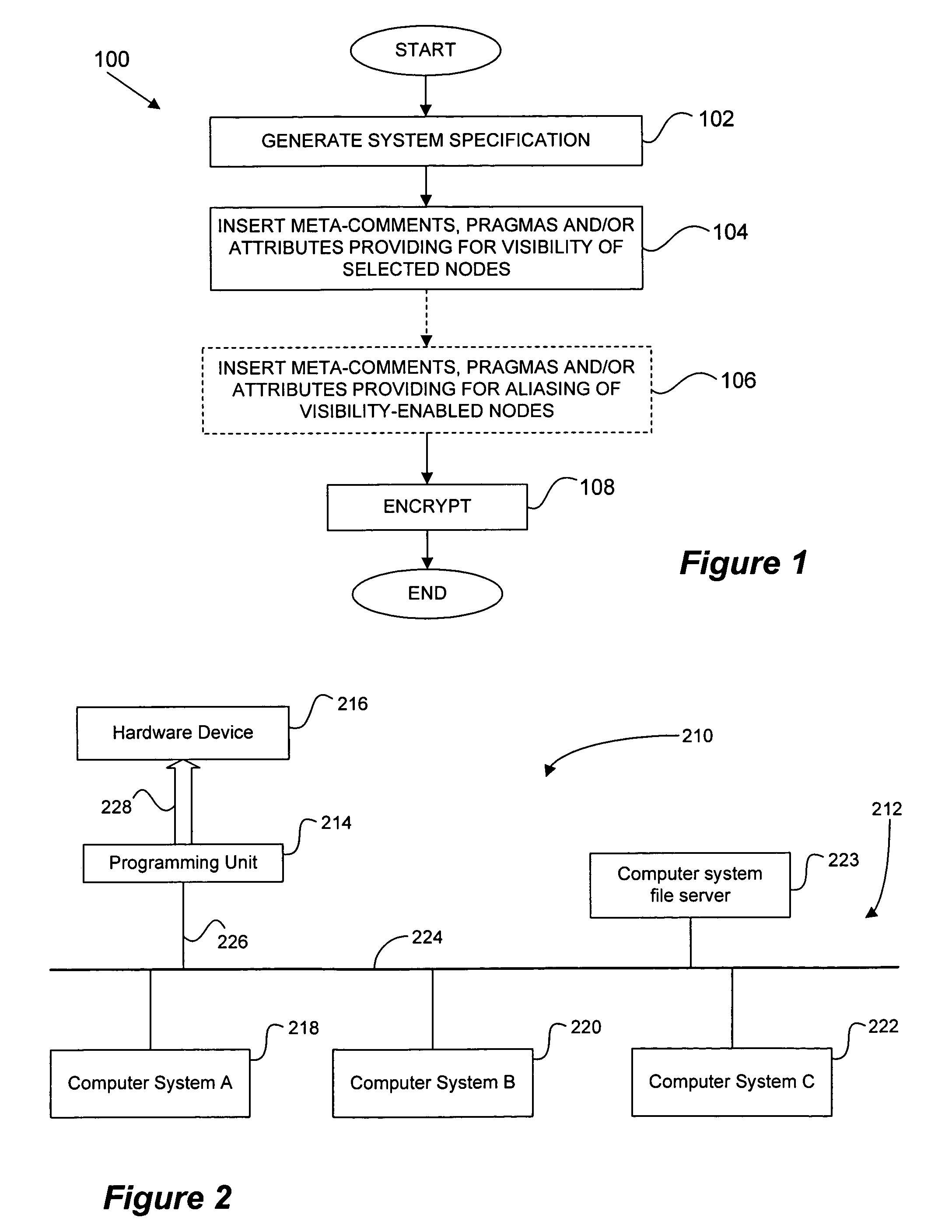
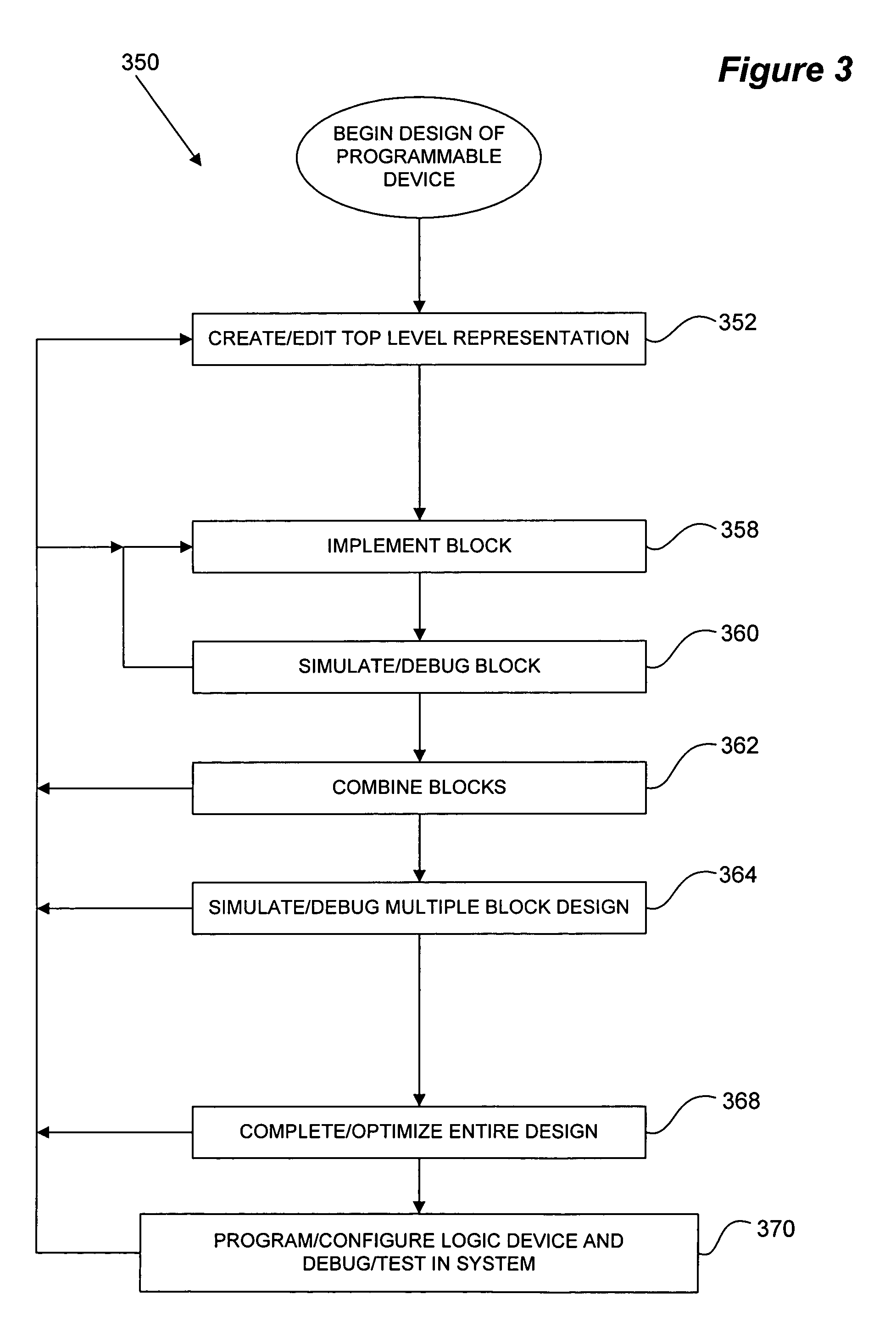
[0026]The following detailed description of the invention will refer to one or more embodiments of the invention, but is not limited to such embodiments. The detailed description is intended only to be illustrative. Those skilled in the art will readily appreciate that the detailed description given herein with respect to the Figures is provided for explanatory purposes as the invention extends beyond these embodiments.

[0027]To develop an electronic design for programming a hardware device (for example, a PLD), a programmable logic development system frequently is used. A design methodology employing pre-existing blocks of IP and the like (typically pre-characterized and parameterizable) can be used to develop a proposed electronic design. For convenience, the following discussion may refer to “integrated circuits” or “PLDs” in addition to hardware devices, though the invention is not limited to any particular type of hardware device, as will be appreciated by those skilled in the a...


PUM


Abstract

Partially opaque intellectual property (IP) includes source code providing the IP functionality. Meta-comments (pragmas or attributes) are provided with the source code to enable visibility of one or more nodes in the IP. Aliasing of the visibility-enabled nodes may also be provided for using meta-comments in the IP source code. The visibility-enabled nodes may be used by system designers in debugging a system design in either a software simulation environment and/or in debugging of a hardware device implementing the partially opaque IP.

Description

BACKGROUND OF THE INVENTION[0001]1. Field of the Invention[0002]This invention relates generally to methods, machine readable media and apparatus for use in connection with testing, evaluating and debugging generally opaque intellectual property (“IP”). More specifically, this invention relates to a technique for providing limited visibility of nodes, signals and other information in encrypted IP.[0003]2. Description of Related Art[0004]In the field of electronics, various electronic design automation (EDA) tools are useful for automating the process by which integrated circuits, multi-chip modules, boards, etc., are designed and manufactured. In particular, electronic design automation tools are useful in the design of standard integrated circuits, custom integrated circuits (e.g., ASICs), and in the design of custom configurations for programmable integrated circuits. Integrated circuits that may be programmable by a customer to produce a custom design for that customer include pr...

Claims


Application Information

Patent Timeline
IPC IPC(8): G06F17/50
CPCG06F17/5054G06F17/5009G06F30/34G06F30/20G06F30/331G06F2117/08G06F30/343G06F2115/08
Inventor FOX, JEFFREY R.SIMPSON, PHILIP A.
Owner TAHOE RES LTD
Why Eureka
Try Eureka