
Organic light emitting display

a light-emitting display and organic technology, applied in the direction of static indicating devices, instruments, semiconductor lamp usage, etc., can solve the problems of the change of the threshold voltage of each drive transistor in the non-uniform crystallization substrate, the inability to obtain desired gray scale, and the unstable quality of the poly-si thin film substrate. , to achieve the effect of preventing the degradation of picture quality

Active Publication Date: 2008-08-12
LG DISPLAY CO LTD
View PDF5 Cites 148 Cited by
  • Summary
  • Abstract
  • Description
  • Claims
  • Application Information

AI Technical Summary

Benefits of technology

The present invention is directed to an organic light emitting display and a method of manufacturing the display that addresses limitations and disadvantages of current technology. The invention provides a unit pixel comprising first to fourth transistors and a capacitor, wherein two of the transistors function as switching devices, one of the transistors functions as a driving device, and one of the transistors functions as a diode device. The invention also provides an organic light emitting display device comprising a plurality of unit pixels, each unit pixel including a first transistor, a second transistor, a third transistor, and a fourth transistor, wherein the fourth transistor has a second threshold voltage to offset the first threshold voltage. The invention also provides a method of manufacturing the organic light emitting display device by forming an organic light emitting display panel including a plurality of unit pixels, each unit pixel including a first transistor, a second transistor, a third transistor, and a fourth transistor, wherein the fourth transistor has a second threshold voltage to offset the first threshold voltage. The technical effects of the invention include preventing degradation of picture quality, improving display quality, and reducing the impact of external factors on display performance.

Problems solved by technology

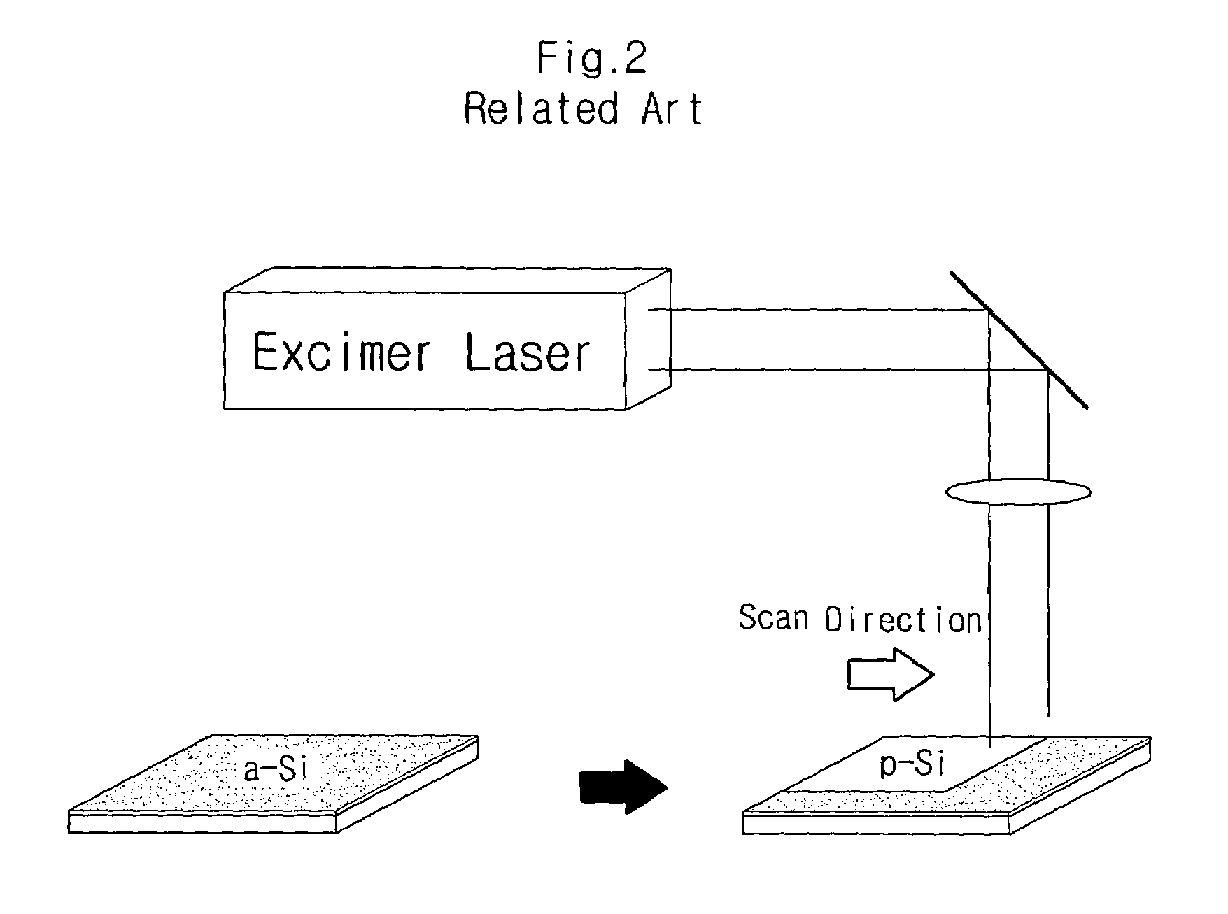
That is, the intensity of the laser power is unstable depending on time and therefore the quality of the poly-Si thin film substrate becomes unstable.
Consequently, a desired gray scale cannot be obtained.
This problem is caused by the change in the threshold voltage of each drive transistor in the non-uniformly crystallized substrate of the display.

Method used


Image

  • Organic light emitting display
  • Organic light emitting display
  • Organic light emitting display

Examples


first embodiment

[0044]FIGS. 4A and 4B are respectively a circuit diagram and a driving waveform of a unit pixel in an AM-type organic light emitting display according to the present invention. Although only a unit pixel is shown in these and subsequent figures, it is understood that an organic light emitting diode display device includes an OLED panel including a plurality of such unit pixels formed in a matrix configuration with a plurality of signal lines provided appropriately as discussed below.

[0045]Referring to FIGS. 4A and 4B, in the unit pixel of the organic light emitting display according to the first embodiment of the present invention, a first transistor T1 has a gate and a drain commonly connected to a first node A1 to thereby act as a diode, and a source connected to a data line supplying a data voltage Vdata. A second transistor T2 has a gate connected to a second select signal line supplying a second select signal Select2, a source connected to the first node A1, and a drain connect...

second embodiment

[0067]In order to address these concerns, a second embodiment is provided as shown in FIGS. 5A and 5B.

[0068]FIGS. 5A and 5B are respectively a circuit diagram and a driving waveform of a unit pixel in an AM-type organic light emitting display according to the second embodiment of the present invention. All the components of the unit pixel in FIG. 5A are operatively coupled.

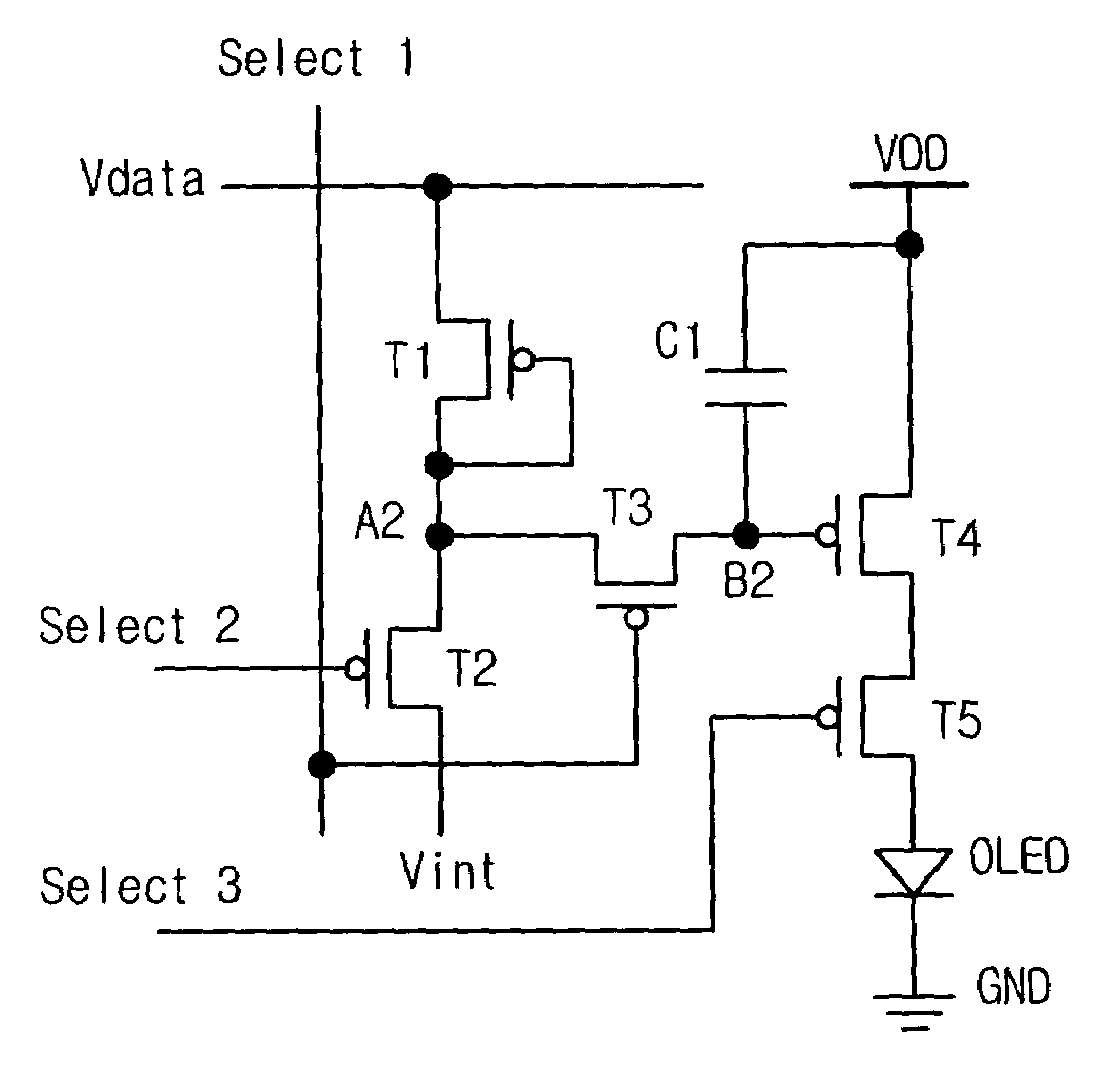
[0069]The second embodiment is similar to the first embodiment. However, a difference is that the second embodiment further includes a fifth transistor T5. That is, the fifth transistor T5 is provided between the fourth transistor T4 and the OLED.

[0070]The fifth transistor T5 has a gate connected to a third select signal line supplying a third select signal Select3, a source connected to the drain of the fourth transistor T4, and a drain connected to the OLED.

[0071]In FIG. 5A, the first to fifth transistors T1 to T5 are PMOS transistors.

[0072]As shown in FIG. 5B, in order for the initialization, the third select s...

third embodiment

[0091]FIGS. 6A and 6B are respectively a circuit diagram and a driving waveform of a unit pixel in an AM-type organic light emitting display according to the present invention. All the components of the unit pixel in FIG. 6A are operatively coupled.

[0092]Referring to FIGS. 6A and 6B, the third embodiment is similar to the second embodiment shown in FIG. 5A, but a difference is that the drain of the second transistor T2 is connected between the fifth transistor T5 and the OLED. Accordingly, the voltage remaining in the OLED can be used as the initialization voltage and no separate initialization voltage line and / or source is needed.

[0093]Since the basic operation of the third embodiment is the same as that of the second embodiment, the following description will be made to highlight the differences.

[0094]The second transistor T2 is turned on in response to the second select signal Select2 of a low level to initialize the unit pixel of the organic light emitting display. Therefore, a ...


PUM


Abstract

An organic light emitting display that is capable of preventing degradation of picture quality, and a method of manufacturing the organic light emitting display are provided. A unit pixel for the organic light emitting display, includes a first transistor coupled to a data line and having a first voltage threshold, a second transistor coupled to the first and third transistors and controlled by a second select signal, a third transistor coupled to the first transistor and controlled by a first select signal, and a fourth transistor coupled to the third transistor and having a fourth voltage threshold such that a drive current of the fourth transistor is controlled independent of the fourth voltage threshold.

Description

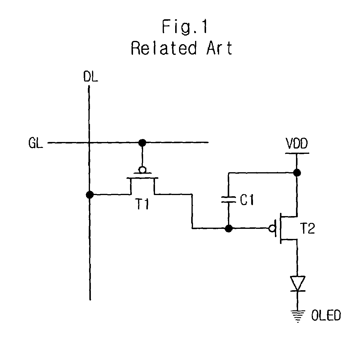
[0001]This application claims the priority benefit of the Korean Patent Application No. 10-2004-0063752 filed on Aug. 13, 2004, which is hereby incorporated by reference.BACKGROUND OF THE INVENTION[0002]1. Field of the Invention[0003]The present invention relates to an organic light emitting display, and more particularly, to an organic light emitting display that can prevent degradation of picture quality and a method of manufacturing the organic light emitting display.[0004]2. Description of the Related Art[0005]An organic light emitting display is a self-luminous display that emits light by electrically exciting fluorescent organic compound, and displays an image by driving N×M organic light emitting diodes (OLEDs).[0006]There are two driving methods for the organic light emitting display, that is, a passive matrix (PM) method and an active matrix (AM) method. In the case of the passive matrix method, anode electrodes and cathode electrodes are formed perpendicular to one another...

Claims


Application Information

Patent Timeline
Patent Type & Authority Patents(United States)
IPC IPC(8): G09G3/30H05B44/00
CPCG09G3/3233H05B33/0896G09G2300/0819G09G2300/0861G09G2310/0251G09G2300/0842H05B45/60Y02B20/30G09G3/30
Inventor HUH, JIN
Owner LG DISPLAY CO LTD
Learn More