Supercharge Your Innovation With Domain-Expert AI Agents!

Printed circuit board with soldering lands

a printed circuit board and soldering lands technology, applied in the direction of sustainable manufacturing/processing, final product manufacturing, non-metallic protective coating applications, etc., can solve the problems of insufficient absorption of accumulated solder in some cases, short circuit between terminals, and high risk of solder spreading, so as to improve yield and improve productivity , the effect of reducing work

Inactive Publication Date: 2008-08-19
FUNAI ELECTRIC CO LTD
View PDF16 Cites 1 Cited by
  • Summary
  • Abstract
  • Description
  • Claims
  • Application Information

AI Technical Summary

Benefits of technology

[0012]The present invention has been established in order to address the above problems and the object thereof is to provide a printed circuit board not requiring an additional space for a dummy land or the like and being capable of preventing short-circuiting between terminals caused by solder buildup.

Problems solved by technology

As a result, when flow soldering is applied, solder is likely to spread excessively at the backside, in the direction of flow, of the land array for multiple terminals and there is a tendency to form a solder buildup and cause short-circuiting between terminals.
Further, JP-A No. 142810 / 2003 discloses the technology that makes short-circuiting hardly occur between terminals by: connecting the land, in a land array for multiple terminals, at the back end in the direction of the flow of flow soldering to a dummy land disposed on the backside of the land in the flow direction through a constricted portion; and making it difficult for the solder once introduced into the dummy land during flow soldering to flow back by the hindrance of the constricted portion.
However, there have been the following problems in the prior technologies explained above.
In the case of a land array for multiple terminals which is used for surface mount and tends to form solder buildup, since the spaces between adjacent terminals are narrow, it is not practical to adopt the technology disclosed in the aforementioned document of Japanese Unexamined Utility Model Publication No. 038663 / 1991 or JP-A No. 290065 / 1998, wherein each land is provided with a dummy land.
In addition, in the case of disposing a dummy land only at the back end, accumulated solder cannot be absorbed sufficiently in some cases.

Method used


Image

  • Printed circuit board with soldering lands
  • Printed circuit board with soldering lands
  • Printed circuit board with soldering lands

Examples


first embodiment

(1) The First Embodiment

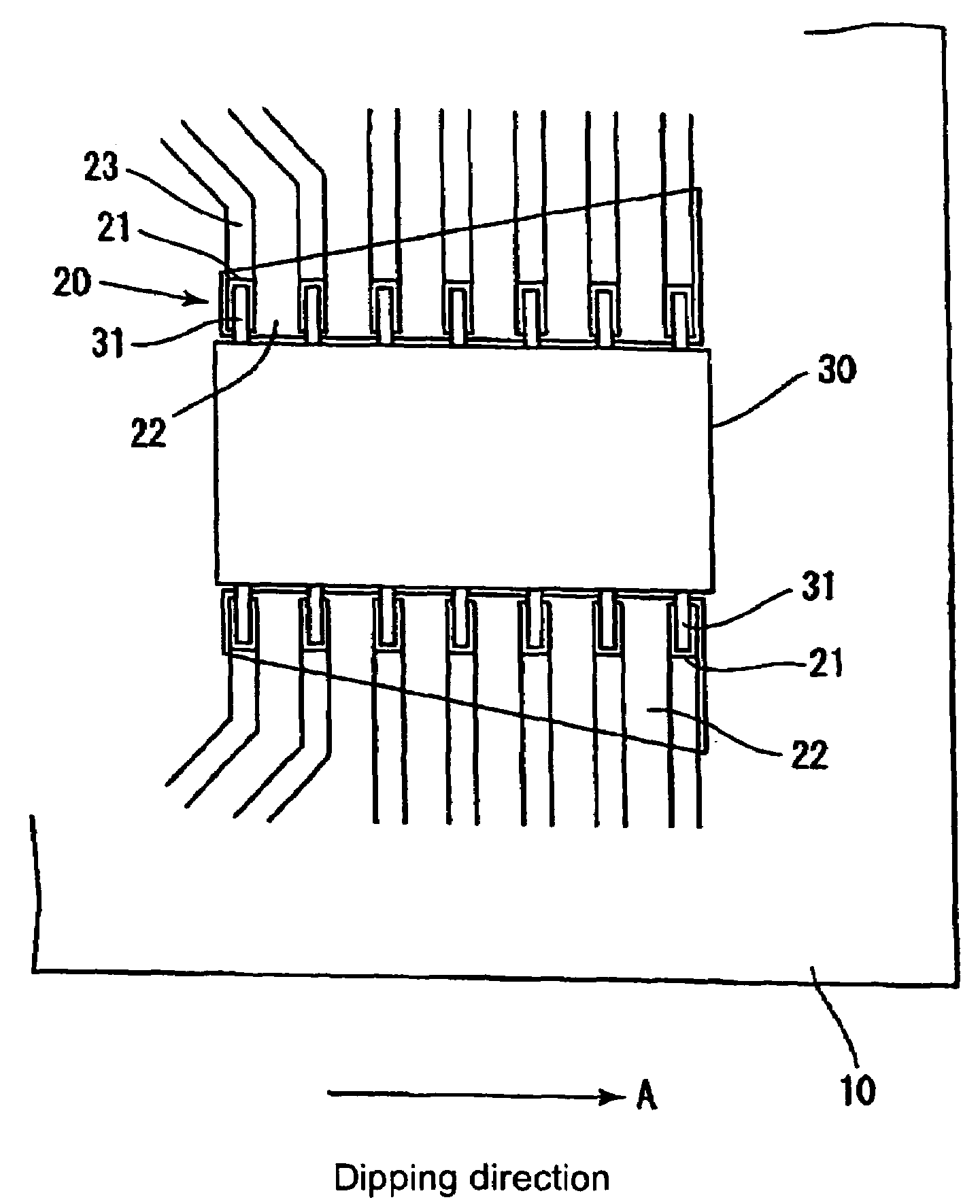
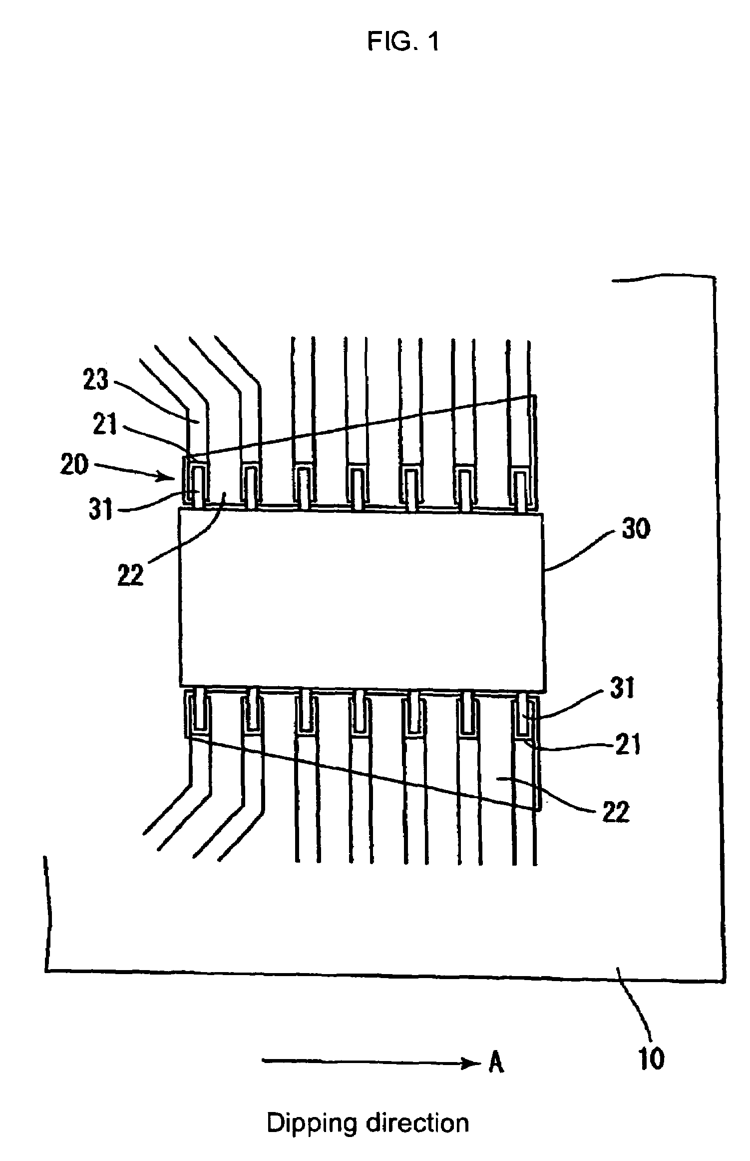
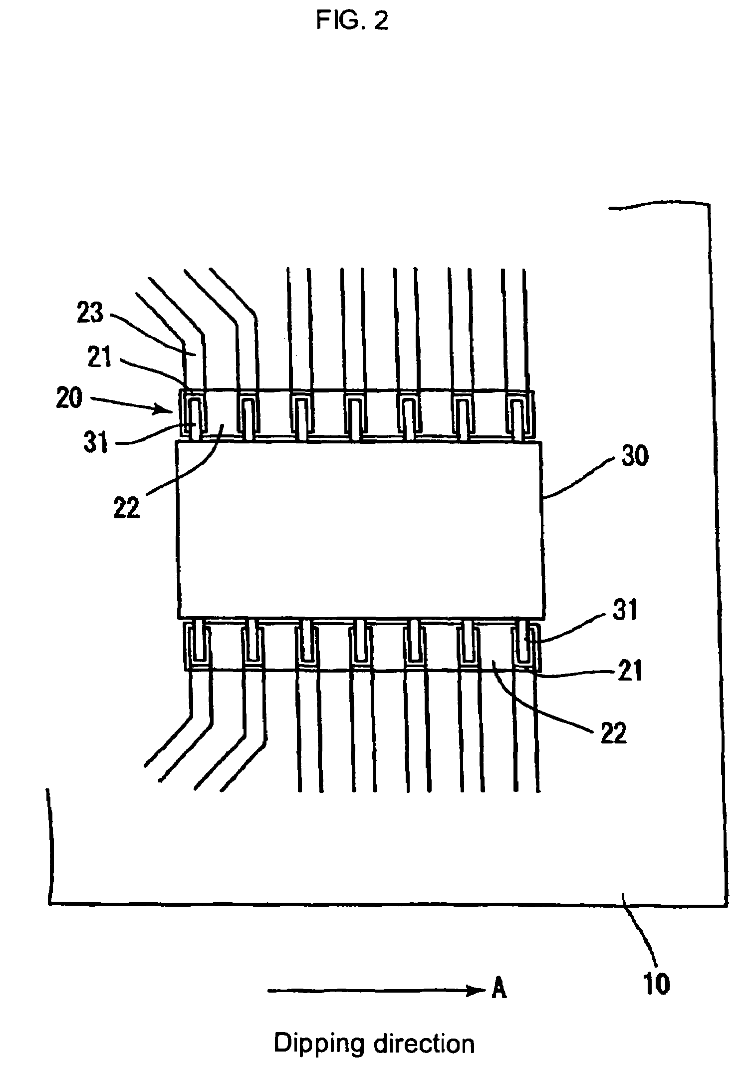
[0050]FIG. 1 is a schematic plan view of a printed circuit board according to the present embodiment.

[0051]In the present embodiment, a printed circuit board 10 has plural land arrays, each of which comprises lands 20 aligned in the dipping direction A, to dip-solder a surface mount IC. A land 20 is composed of: a land pattern 21 of a rectangular shape having the narrow side in the dipping direction; and a non-resist portion 22 formed by exfoliating a resist with which the pattern layer is covered at the portion touching a terminal 31 so as to be larger than the land pattern 21 from the top to the end of a land array. A wiring pattern 23 extends from each land pattern 21 toward the outside of an IC package 30 in the direction perpendicular to the dipping direction A.

[0052]The non-resist portion 22 has a trapezoidal shape; the width thereof is the distance from the front end to the back end of the land pattern array in the dipping direction A and the length th...

second embodiment

(2) The Second Embodiment

[0060]FIG. 3 is a schematic plan view of a printed circuit board according to the present embodiment. The example of a modification of a non-resist portion 22 in the above first embodiment is explained.

[0061]In the present embodiment, a printed circuit board 110 has plural land arrays, each of which comprises lands 120 aligned in the dipping direction A, to dip-solder a surface mount IC. A land 120 is composed of: a land pattern 121 of a rectangular shape having the narrow side in the dipping direction; and a non-resist portion 122 formed by exfoliating a resist with which the pattern layer is covered at the portion touching a terminal 131 so as to be larger than the land pattern 121. A wiring pattern 123 extends from each land pattern 121 toward the outside of an IC package 130 in the direction perpendicular to the dipping direction A.

[0062]The non-resist portion 122 has a step-like shape; the width thereof is the distance from the front end to the back end...

third embodiment

(3) The Third Embodiment

[0066]FIG. 4 is a schematic plan view of a printed circuit board according to the present embodiment as the example of a modification of a non-resist portion 22.

[0067]In the present embodiment, a printed circuit board 210 has plural land arrays, each of which comprises lands 220 aligned in the dipping direction A, to dip-solder a surface mount IC. In the aforementioned first and second embodiments, the area of the non-resist portion 22 at each land is expanded from the front side to the backside in the predetermined direction. However, as long as excessive molten solder does not remain at the back end land 220 in a land array, it is not always necessary to expand the area of the non-resist portion 22 at the back end land 220 or to commence expanding the area of the non-resist portion 22 from the front end land. The position where the area of a non-resist portion 22 is expanded may be anywhere so long as the position is somewhere in the region of the land arra...


PUM


Abstract

The present invention provides a printed circuit board having an area of non-resist portion, where each non-resist portion expands gradually toward the back end of a land array in the dipping direction A. Thus the area of solder deposition also expands in the region of the land array, thereby excessive solder does not remain up to the back end of the land array, and resultantly the amount of solder buildup at the backside in the dipping direction A can be reduced. Further, the present invention makes it unnecessary to dispose a dummy land for the prevention of solder buildup at the backmost portion of the land array, and thus the space used for a dummy land can be utilized effectively.

Description

BACKGROUND OF THE INVENTION[0001]1. Field of the Invention[0002]The present invention relates to a printed circuit board having land arrays to which solder is applied by flow soldering when an electronic part, in particular an element having plural terminals aligned in a line like an IC, is mounted thereon.[0003]2. Description of the Prior Art[0004]In the case of a land array for multiple terminals on a conventional printed circuit board, on which a surface mount IC element having plural terminals aligned in parallel is mounted by dip soldering, the length of the exposed portion, not covered with a resist, of each land has heretofore been identical. As a result, when flow soldering is applied, solder is likely to spread excessively at the backside, in the direction of flow, of the land array for multiple terminals and there is a tendency to form a solder buildup and cause short-circuiting between terminals.[0005]With regard to the problem, Japanese Unexamined Utility Model Publicati...

Claims


Application Information

Patent Timeline
Patent Type & Authority Patents(United States)
IPC IPC(8): H05K3/34H01L23/48H05K3/28
CPCH05K3/3421H05K3/3452H05K3/3468H05K2203/046H05K2201/0989H05K2201/10689Y02P70/50
Inventor URISU, TAKAYOSHI
Owner FUNAI ELECTRIC CO LTD
Features
  • R&D
  • Intellectual Property
  • Life Sciences
  • Materials
  • Tech Scout
  • Unparalleled Data Quality
  • Higher Quality Content
  • 60% Fewer Hallucinations
Learn More