
Power control circuit, semiconductor device and transceiver circuit using the same

a power control circuit and semiconductor technology, applied in the direction of gain control, digital transmission, baseband system details, etc., can solve the problems of insufficient stability and accuracy, inability to avoid degradation of the output signal of the transmitted power amplifier, and limit to a communication system, so as to reduce the size and cost of the communication device, stable high-speed operation, and the effect of stable high-speed operation

Active Publication Date: 2008-08-19
RENESAS ELECTRONICS CORP
View PDF14 Cites 9 Cited by
  • Summary
  • Abstract
  • Description
  • Claims
  • Application Information

AI Technical Summary

Benefits of technology

[0015]According to another aspect of the present invention, for achieving the above object, there is provided a semiconductor device comprising: a circuit block including, a receiver circuit which amplifies a received first signal; a first frequency conversion circuit which converts the frequency of the first signal of post-amplification outputted from the receiver circuit to output a second signal; a second frequency conversion circuit which inputs a third signal to be transmitted and converts the frequency of the third signal to output a fourth signal; a first amplifier which amplifies the fourth signal outputted from the second frequency conversion circuit and whose gain is controlled by a second power control signal; and the above-mentioned power control circuit which controls output power of an external second amplifier amplifying the fourth signal by use of a first power control signal in such a manner that the output power reaches a desired power value, wherein the circuit block is formed over the same semiconductor substrate. The semiconductor device having the above configuration is equipped with the power control circuit which can be shared among a plurality of frequency bands and a plurality of systems because it is capable of stable high-speed operation. Thus, the use of the semiconductor device of the present invention allows realization of reductions in size and cost of a communication device such as a multi-band / multi-mode-capable cellular phone or the like.
[0016]According to a further aspect of the present invention, for attaining the above object, there is provided a transceiver circuit comprising: a circuit block including, a first receiver circuit which amplifies a 1 ath signal of a first communication system, which is received by an antenna; a second receiver circuit which amplifies a 1 bth signal of a second communication system, which is received by the antenna; a first frequency conversion circuit which converts the frequency of the 1 ath or 1 bth signals of post-amplification outputted from the first or second receiver circuits to thereby output a second signal; a second frequency conversion circuit which inputs a 3 ath signal to be transmitted of the first communication system or a 3 bth signal to be transmitted of the second communication system and executes frequency conversion to the same to thereby output a fourth signal; a first amplifier which amplifies the fourth signal outputted from the second frequency conversion circuit and whose gain is controlled by a second power control signal; a second amplifier which power-amplifies the fourth signal of post-amplification outputted from the first amplifier; a detector which detects a power value of an output signal of the second amplifier to output a detected signal; and the above-mentioned power control circuit which controls an output power of the second amplifier by use of a first power control signal in such a manner that the output power reaches a desired power value. The transceiver circuit having the above configuration is equipped with the power control circuit capable of being shared for a plurality of frequency bands and a plurality of systems because it is capable of stable high-speed operation. Accordingly, the use of the transceiver circuit of the present invention allows realization of reductions in size and cost of a communication device such as a multi-band / multi-mode-adaptable cellular phone or the like.

Problems solved by technology

In the technique disclosed in the patent document 1, a feedback circuit is susceptible to temperature changes and a variation in power supply because it is constituted of an analog circuit, and hence stability and accuracy thereof become insufficient unavoidably.
As a result, it is not possible to avoid degradation of the output signal of the transmitted power amplifier.
Thus, there is a limit to a communication system to which the present technique is applicable.
In the technique disclosed in the patent document 2, a sample hold leak (phenomenon that varies in voltage for holding a capacitor due to the leak of an electrical charge of a capacitor constituting a sample and hold circuit) occurs because the sample and hold circuit is similarly realized by an analog circuit, so that it is difficult to hold the output signal of the power amplifier at a constant value.
When, however, high-speed power control in a burst mode such as GSM (Global System for Mobile Communication) or the like being in widespread use in Europe is performed, there is a possibility that a feedback circuit will be brought into in stabilization or oscillations because the phase of a feedback signal corresponding to a clock frequency is turned 180° due to a clock delay contained in the digital signal processing.

Method used


Image

  • Power control circuit, semiconductor device and transceiver circuit using the same
  • Power control circuit, semiconductor device and transceiver circuit using the same
  • Power control circuit, semiconductor device and transceiver circuit using the same

Examples


first preferred embodiment

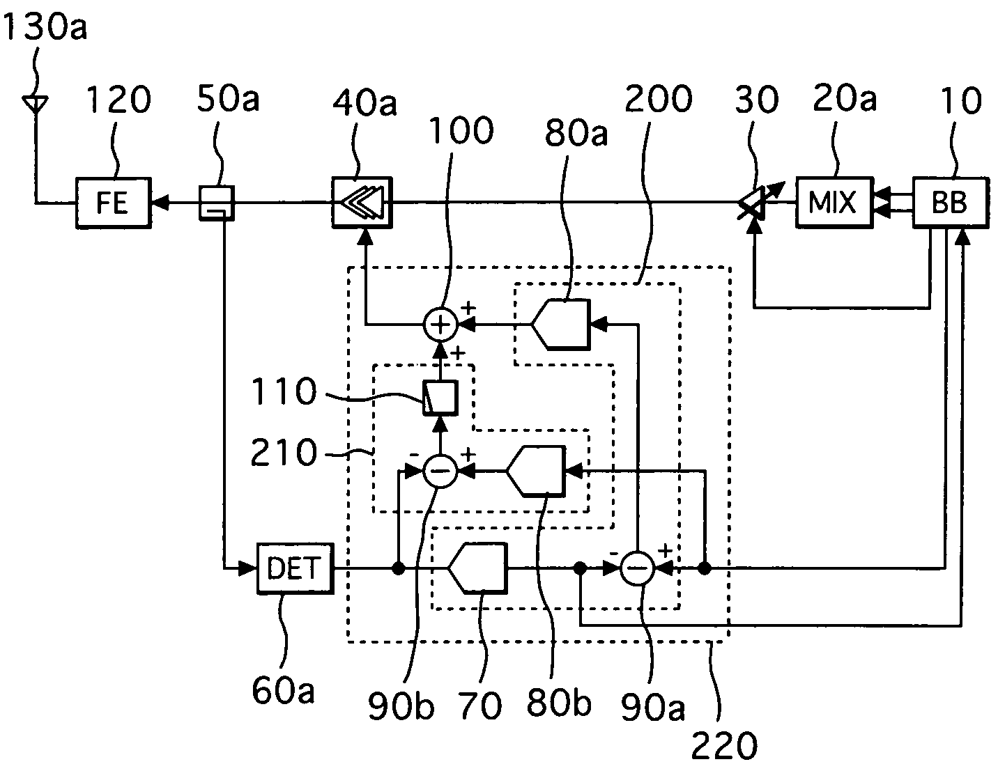
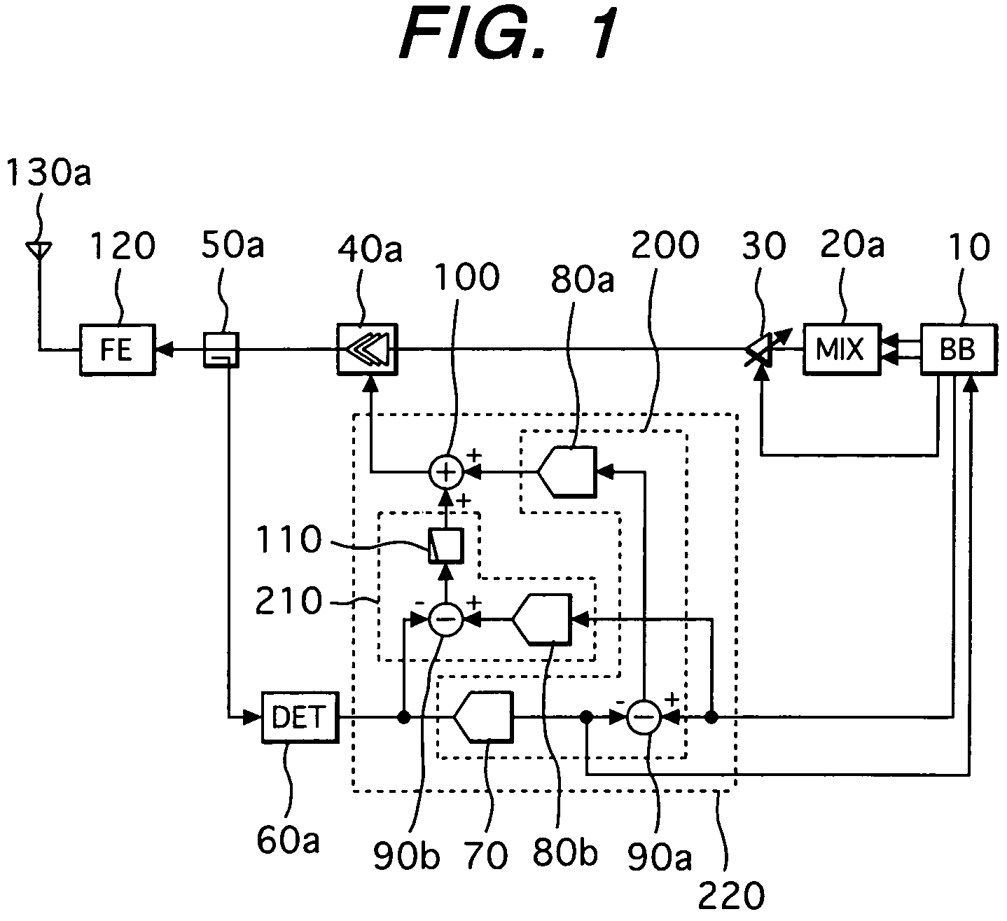
[0043]A first embodiment illustrative of a power control circuit of the present invention is shown in FIG. 1. As one example, a case is indicated, in which the present invention is applied to a cellular phone appropriate to GSM and W-CDMA, in order to simply describe the structure, operation and effects of the power control circuit according to the present embodiment. FIG. 1 is a circuit configuration diagram showing a transmitter block of a cellular phone equipped with the power control circuit according to the present embodiment.

[0044]In FIG. 1, reference numeral 10 indicates a base band signal processor (BB), reference numeral 20a indicates a frequency conversion circuit (MIX), reference numeral 30 indicates an available gain amplifier, reference numeral 40a indicates a power amplifier, reference numeral 50a indicates a directional coupler, reference numeral 60a indicates a detector (DET), reference numeral 70 indicates an analog to digital (A / D) converter, reference numerals 80a...

second preferred embodiment

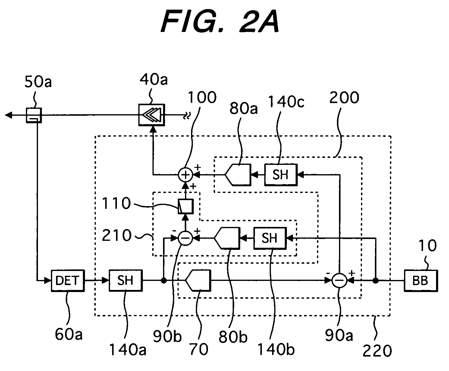
[0053]A second embodiment illustrative of a power control circuit of the present invention is shown in FIG. 2A. FIG. 2A is a circuit configuration diagram showing a transmitter block of a cellular phone equipped with the power control circuit according to the present embodiment. The cellular phone, to which the present invention is applied, corresponds even to EDGE in addition to GSM and W-CDMA. Thus, the power control circuit according to the present embodiment is applied to GSM and EDGE modes and serves as a multi-mode power control circuit.

[0054]When the transmitter block performs the EDGE mode, its basic operation is similar to the GSM mode in the first embodiment. Points different from the GSM mode will next be explained.

[0055]FIG. 3 is a graph showing time responses of a transmitted signal power value transmitted from an antenna 130a and normalized time masks where GSM and EDGE modes are performed.

[0056]In FIG. 3, the horizontal axis indicates time, and the vertical axis indic...

third preferred embodiment

[0074]A third embodiment illustrative of a power control circuit of the present invention is shown in FIG. 7. FIG. 7 is a circuit configuration diagram showing a transmitter block of a cellular phone equipped with the power control circuit according to the present embodiment. The cellular phone to which the present invention is applied, is adapted to each of GSM, W-CDMA and EDGE in a manner similar to the second embodiment. The power control circuit according to the present embodiment is used where a comparator 90b can be turned OFF during the modulated signal output period 450. Only a sample and hold circuit 140c is disposed on the input side of an A / D converter 80a. Thus, as compared with the second embodiment, the power control circuit 220 is reduced in size by a reduction in the number of sample and hold circuits.

[0075]A basic operation of the power control circuit 220 adapted to GSM and EDGE is similar to the second embodiment but the operation of the sample and hold circuit in...


PUM


Abstract

There is provided a power control circuit having a stable high-speed operation, and a semiconductor device and a transceiver circuit using it. The power control circuit controls the gain of an amplifier so that power outputted from the amplifier reaches a desired value according to a digital control signal. The power control circuit includes a digital feedback loop which converts a detected signal obtained by detecting a value of the output power of the amplifier to a digital signal, determines a differential between the digital signal and the digital control signal, converts the differential to an analog signal and outputs a first feedback signal, an analog feedback loop which outputs a high frequency element corresponding to a differential between an analog signal to which the digital control signal is converted and the detected signal, as a second feedback signal, and an adder which determines the sum of the first and the second feedback signal and outputs a gain control signal for controlling the gain of the amplifier.

Description

CLAIM OF PRIORITY[0001]The present patent application claims priority from Japanese application JP 2004-337266 filed on Nov. 22, 2004, the content of which is hereby incorporated by reference into this application.FIELD OF THE INVENTION[0002]The present invention relates to a technique which controls output power at a mobile wireless communication terminal or wireless communication devices such as a transmitter of a base station for wireless communication, etc., and particularly to a power control circuit suitable for application to wireless communication devices adapted to a plurality of frequency bands and a plurality of systems.BACKGROUND OF THE INVENTION[0003]A mobile communication system typified by a cellular phone has been increased in penetration on a global scale. Several communication systems have been used according to the locality. As one of important techniques used in the mobile communication system, there is known a technique called APC (Auto Power Control) which cont...

Claims


Application Information

Patent Timeline
Patent Type & Authority Patents(United States)
IPC IPC(8): H04B1/04H01Q11/12
CPCH03G3/02H03G3/3047H03G3/3042
Inventor KURIYAMA, AKIRATANAKA, SATOSHI
Owner RENESAS ELECTRONICS CORP
Learn More