High-temperature superconducting device and manufacturing method thereof

a superconducting device and high-temperature technology, applied in the direction of superconductor devices, semiconductor devices, electrical devices, etc., can solve the problems of no longer being fulfilled, circuits cannot be operated, and generating parasitic inductance, etc., to achieve stable high-speed operation

Inactive Publication Date: 2006-11-02
FUJITSU LTD +1
View PDF12 Cites 4 Cited by
  • Summary
  • Abstract
  • Description
  • Claims
  • Application Information

AI Technical Summary

Benefits of technology

[0027] It is an object of the present invention to allow a stable high-speed operation of a superconductor circuit such as an SFQ circuit.
[0031] By separately fabricating at least the two ramp-edge Josephson junctions 9 and 10 whose critical current densities Jc differ to each other above the substrate 1, and by utilizing each performance of the junctions differently depending on each element circuit, both a high-speed operation and a stable operation of the superconducting circuit device such as a SFQ circuit can be realized. Consequently, the performance of the high-temperature superconducting device can be enhanced.
[0032] In the above case, a Josephson junction 9 having a relatively high critical current density is used so that Ic×Rn is made larger, allowing a high-speed operation, while a Josephson junction 10 having a relatively low critical current density is used so that the junction width is widened and the inductance L is reduced, allowing a stable operation in a manner which fulfills the condition of L×Ic<φo in a circuit element having a strict L×Ic condition.
[0035] In such an element circuit, in order to make the product of L×Ic higher, it is possible to narrow the junction width so that Jc can be made higher without being restricted by the L×Ic product condition.
[0036] That is to say, it is important that junctions with different performances are used separately, in such a manner that an element circuit requiring high speed and high precision should contain a high-Jc junction, while an element circuit requiring a strict condition on the product of L×Ic should include a relatively low Jc junction so that the parasitic inductance L can be reduced.

Problems solved by technology

However, in the ramp-edge structure, in which a barrier layer is sandwiched by the upper and lower electrodes through the bridge portion, parasitic inductance is generated in series with the junction.
Hence, the above-described condition for the product of L×Ic (L×Ico) can no longer be fulfilled, and the circuit cannot be operated.
However, if the junction width is widened in order to reduce the parasitic inductance influence as much as possible, Jc of the Josephson junction cannot be made higher, so that the junction with relatively small-value product of Ic×Rn has to be used.
Consequently, the SFQ pulse width becomes wider, and a problem is caused in which the circuit performance is deteriorated in such a manner that the operational speed of the SFQ circuit is restricted, or the operational uncertainty (jitter) becomes greater.

Method used


Image

  • High-temperature superconducting device and manufacturing method thereof
  • High-temperature superconducting device and manufacturing method thereof
  • High-temperature superconducting device and manufacturing method thereof

Examples


first embodiment

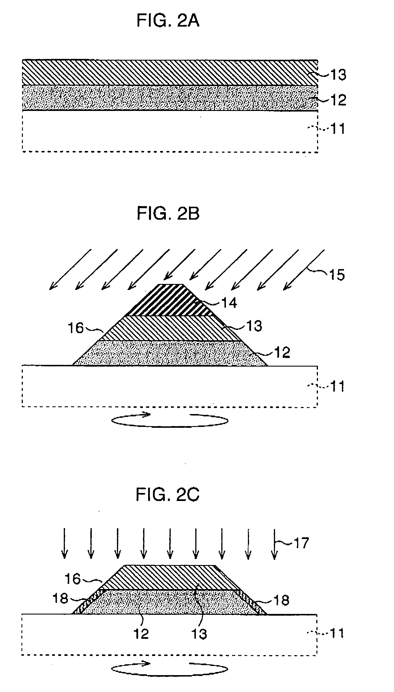
[0060] Hereinafter, a forming process of an interface-engineered ramp-edge junction according to the present invention is explained with reference to FIGS. 2A to 4B.

[0061] First, as shown in 2A, a laser deposition method (PLD: pulse laser deposition) is used to sequentially deposit a lower electrode layer 12 formed of YBCO (YBa2Cu3O7-x) having a thickness of 200 nm for example, and an insulating layer 13 formed of a LSAT having a thickness of 300 nm for example, on a LSAT substrate 11 formed of [LaAlO3]0.3[Sr(Al,Ta)O3]0.7.

[0062] Next, as shown in 2B, a photo-resist is coated on the insulating layer 13, which is then exposed and developed. After that, the photo-resist film is reflowed by baking, so that a photo-resist pattern 14 is formed. The photo-resist pattern 14 is then used as a mask, so as to irradiate argon ion 15 from a diagonal direction with the LSAT substrate 11 rotated such that the insulating layer 13 and the lower electrode layer 12 are etched, resulting in formation ...

second embodiment

[0068] Next, with reference to FIGS. 5A to 6B, a forming process of an interface-engineered ramp-edge junction according to the present invention will be explained.

[0069] First, as shown in FIG. 5A, as with the above-described first embodiment, a laser deposition method is used to sequentially deposit on a LSAT substrate a lower electrode layer 12 formed of YBCO (YBa2Cu3O7-x) having a thickness of 200 nm for example, and an insulating layer 13 formed of LSAT having a thickness of 300 nm for example.

[0070] Subsequently, a photo-resist is coated on the insulating layer 13, which is then exposed and developed. The photo-resist film is then reflowed by baking, so that a photo-resist pattern 14 is formed. The photo-resist pattern 14 is then used as a mask, so as to irradiate argon ion 15 from a diagonal direction with the LSAT substrate 11 rotated, such that the insulating layer 13 and the lower electrode layer 12 are etched, resulting in formation of a ramp slope 16.

[0071] As shown in...

third embodiment

[0075] With the above-described conditions as premises, a superconducting circuit device according to the present invention will be explained next.

[0076]FIG. 7 shows an equivalent circuit diagram of a DC / SFQ conversion circuit, which is one example of a pulse generating circuit, the pulse generating circuit being a basis of the superconducting circuit device in the third embodiment of the present invention.

[0077] The circuit applies normal electrical signal used in semiconductor circuits through an input Isgn, and an SFQ pulse is outputted from an output terminal when an input signal exceeds a certain threshold level, where, the larger is the product of Ic×Rn of a Josephson junction used in the circuit, the narrower the time width of the generated pulse becomes. This state will be explained with reference to FIG. 8.

[0078]FIG. 8 shows simulation results of generated pulses where the product of Ic×Rn is set to 0.5 mV, 1.0 mV, and 1.5 mV.

[0079] The half widths of the pulses are 5.8 ...


PUM


Abstract

At least two ramp-edge-structure Josephson junctions having different critical current densities to one another are provided on a substrate.

Description

CROSS-REFERENCE TO RELATED APPLICATIONS [0001] This application is based upon and claims the benefit of priority from the prior Japanese Patent Application No. 2003-089776, filed on Mar. 28, 2003, the entire contents of which are incorporated herein by reference. BACKGROUND OF THE INVENTION [0002] 1. Field of the Invention [0003] This invention relates to a high-temperature superconducting device and a manufacturing method thereof and, more particularly, to a high-temperature superconducting device characterized by a means to form the high-temperature superconducting device by a ramp-edge-type superconductor junction with various critical current densities Jc, and a manufacturing method thereof. [0004] 2. Description of the Related Art [0005] In recent years, oxide high-temperature superconductors as typified by yttrium-type superconductors have been expected to be applied to various fields such as sensors and logic circuits, since their superconducting state is exhibited at a tempe...

Claims


Application Information

Patent Timeline
Patent Type & Authority Applications(United States)
IPC IPC(8): H01L39/22H01L29/06H01L27/18H01L39/24
CPCH01L39/2496H01L27/18H10N69/00H10N60/0941
Inventor HORIBE, MASAHIROSUZUKI, HIDEOISHIMARU, YOSHIHIROWAKANA, HIRONORITANABE, KEIICHI
Owner FUJITSU LTD
Why Eureka
Try Eureka