Semiconductor storage device incorporated into a system LSI with finer design rules

a technology of design rules and semiconductors, applied in the field of semiconductor storage devices incorporated into systems lsi with finer design rules, can solve the problems of difficult high-speed operation and low threshold voltage, and achieve the effects of stable high-speed operation, suppressing an increase in circuit size, and high reliability

Active Publication Date: 2010-06-08
CETUS TECH INC
View PDF12 Cites 13 Cited by
  • Summary
  • Abstract
  • Description
  • Claims
  • Application Information

AI Technical Summary

Benefits of technology

[0014]The present invention is devised to solve the conventional problem. An object of the present invention is to provide a semiconductor storage device which can suppress an increase in circuit size and achieve a stable high-speed operation while allowing constituent transistors to have sufficient operating capabilities, even when the semiconductor storage device is incorporated into a system LSI with finer design rules.
[0016]As described above, according to the present invention, the word lines at a high voltage can be operated at high speeds with high reliability in response to a control signal from the control circuit at a low voltage by a transistor circuit which is disposed between the control circuit and the word lines and includes a gate oxide film having a thickness between the thicknesses of the gate oxide film of the control circuit and the word lines.
[0017]Thus even when the semiconductor storage device is incorporated into a system LSI with finer design rules, it is possible to suppress an increase in circuit size and achieve a stable high-speed operation while allowing constituent transistors to have sufficient operating capabilities.

Problems solved by technology

Thus the threshold voltage is not sufficiently high.
Thus it is difficult to perform high-speed operations.

Method used


Image

  • Semiconductor storage device incorporated into a system LSI with finer design rules
  • Semiconductor storage device incorporated into a system LSI with finer design rules
  • Semiconductor storage device incorporated into a system LSI with finer design rules

Examples


Embodiment Construction

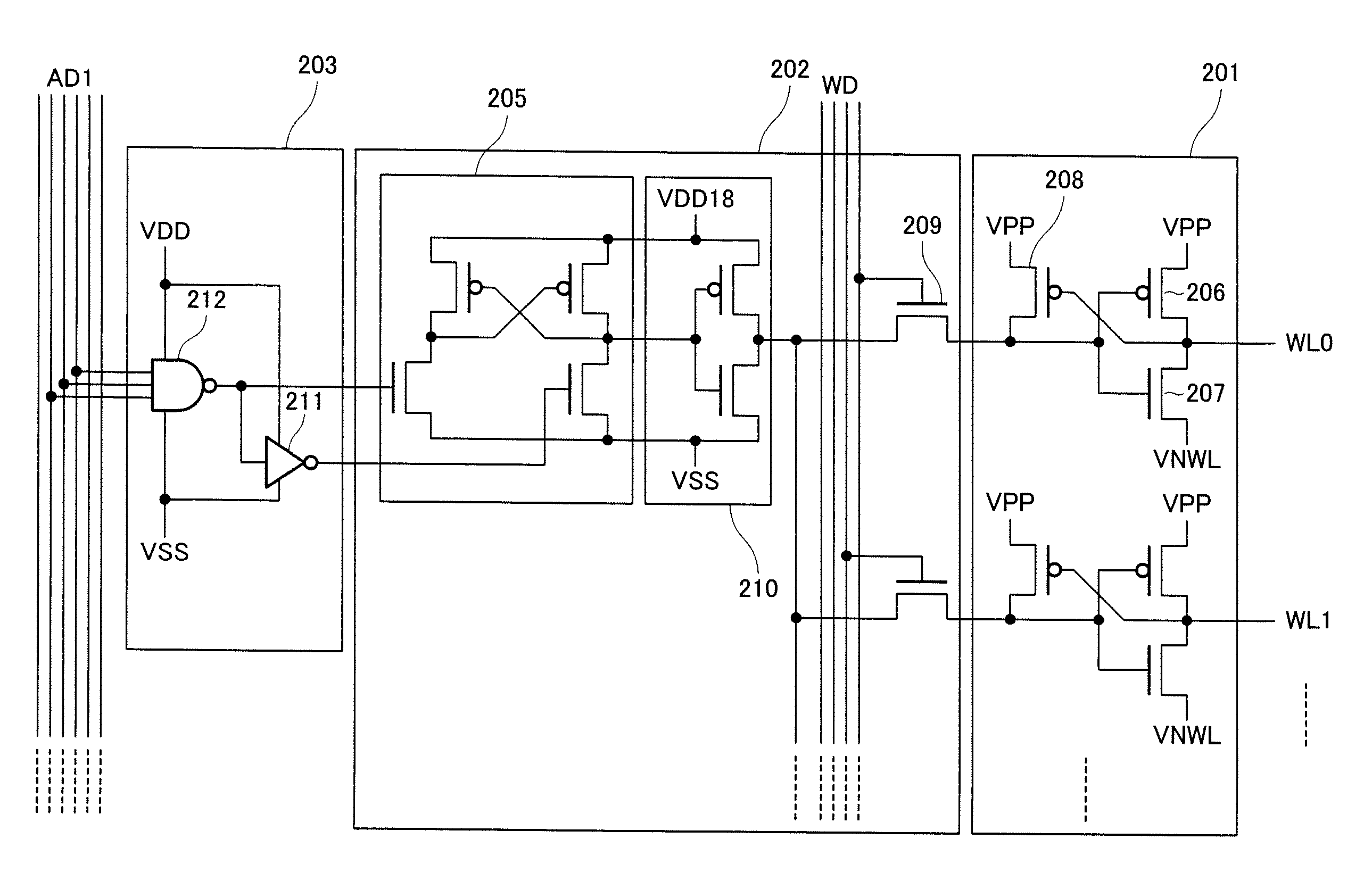
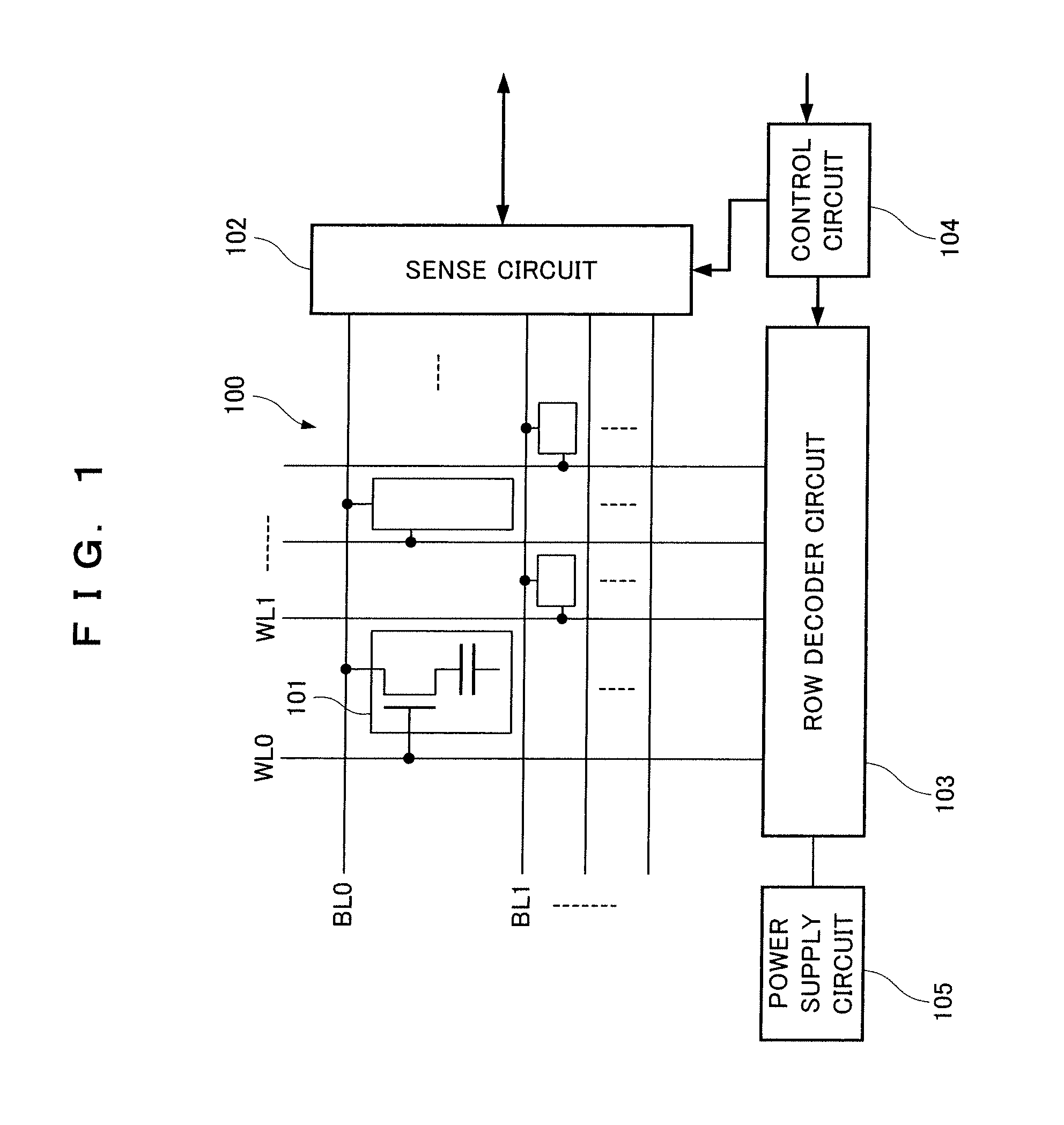
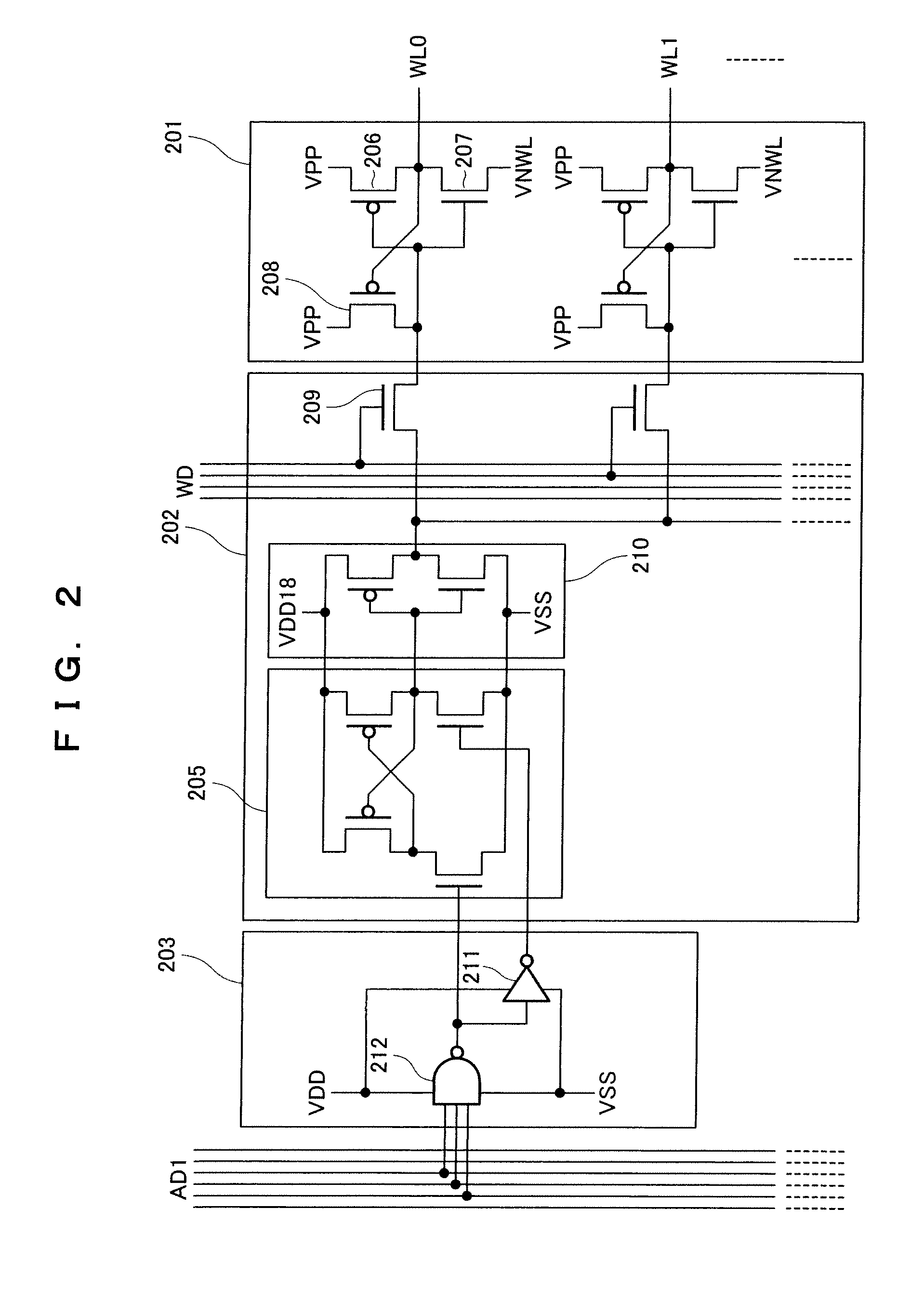
[0023]A first configuration of a semiconductor storage device according to an embodiment of the present invention includes, as a basic concept, memory cells, word lines connected to the memory cells, a row decoder circuit connected to the word lines, and a control circuit for controlling the access of the row decoder circuit to the memory cells through the word lines, wherein the control circuit is made up of a transistor in which a gate oxide film has a first thickness, and the row decoder circuit is made up of a transistor in which the gate oxide film has the first thickness, a transistor in which the gate oxide film has a second thickness larger than the first thickness, and a transistor in which the gate oxide film has a third thickness larger than the second thickness.

[0024]With this configuration, the word lines at a high voltage can be quickly operated with high reliability in response to a control signal from the control circuit at a low voltage by a transistor circuit which...


PUM


Abstract

In the present invention, a row decoder circuit is made up of a transistor having a first gate oxide film thickness, a transistor having a second gate oxide film thickness, and a transistor having a third gate oxide film thickness. Thus even a control circuit at a lower voltage can drive word lines at high speeds while achieving reliability.

Description

FIELD OF THE INVENTION[0001]The present invention relates to a semiconductor storage device incorporated into a system LSI with finer design rules.BACKGROUND OF THE INVENTION[0002]Conventionally, semiconductor storage devices incorporated into system LSIs with finer design rules (for example, see Japanese patent laid-open publications including Japanese Patent Laid-Open No. 7-307091 and Japanese Patent Laid-Open No. 2002-298579) are configured as shown in FIG. 4.[0003]FIG. 4 is a block diagram showing the configuration of a conventional semiconductor storage device. In FIG. 4, reference numeral 1 denotes a memory cell, reference numeral 2 denotes a sense circuit, reference character WL denotes a word line, reference character BL denotes a bit line, reference numeral 3 denotes a row decoder circuit, and reference numeral 4 denotes a level shifter.[0004]The memory cell 1 is a typical DRAM memory cell. In order to charge a capacitor from an N-channel transistor, a voltage higher than t...

Claims


Application Information

Patent Timeline
Patent Type & Authority Patents(United States)
IPC IPC(8): G11C11/00
CPCG11C8/08G11C11/4087G11C11/4085G11C8/10
Inventor ORIGASA, KENICHI
Owner CETUS TECH INC
Why Eureka
Try Eureka