

Display panel and display device having the panel
a display panel and display device technology, applied in static indicating devices, non-linear optics, instruments, etc., can solve problems such as difficulty in reducing frame area, and achieve the effect of simplifying the production process of liquid crystal display panels
- Summary
- Abstract
- Description
- Claims
- Application Information
AI Technical Summary
Benefits of technology
Problems solved by technology
Method used
Image

Examples
embodiment 1
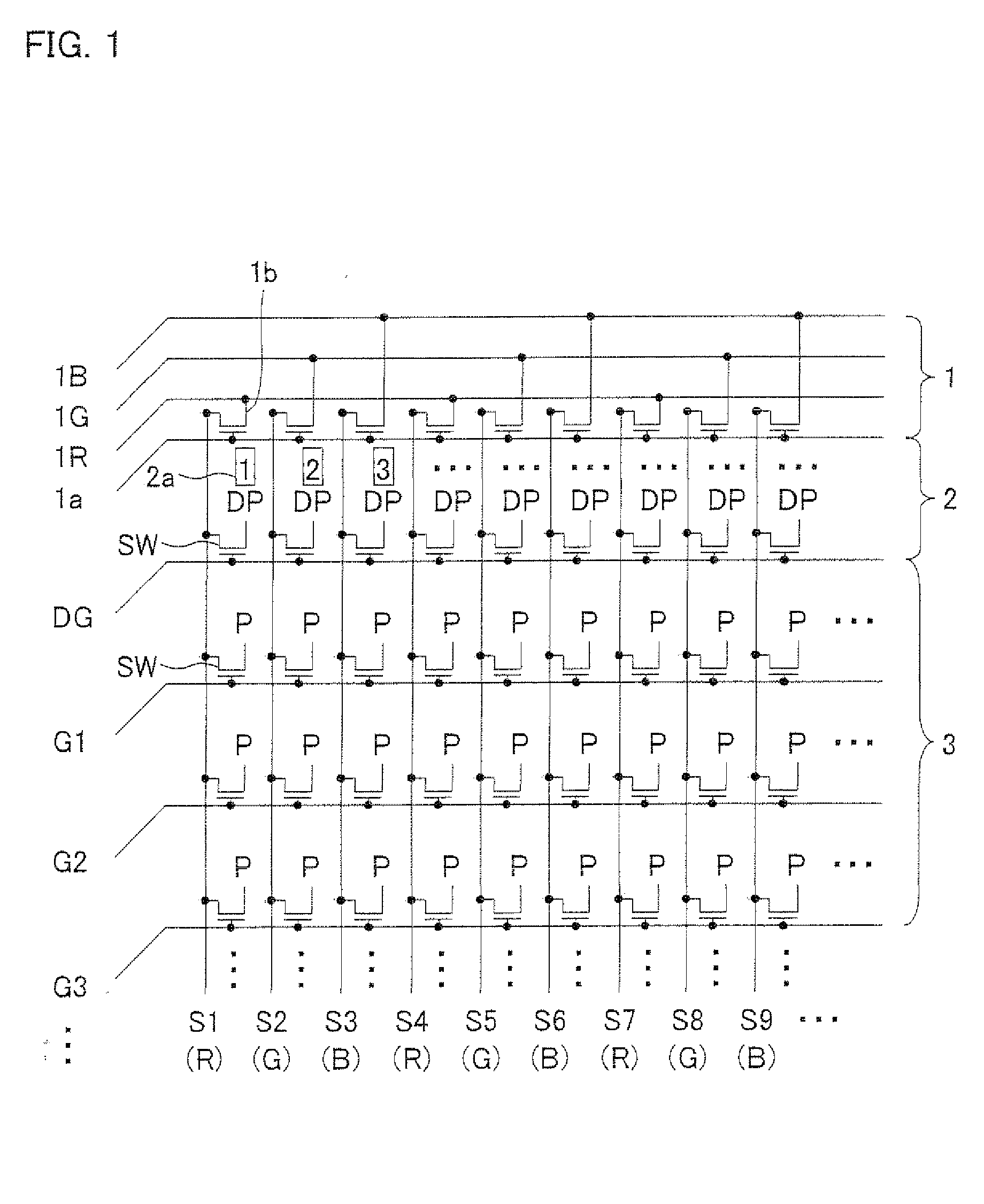
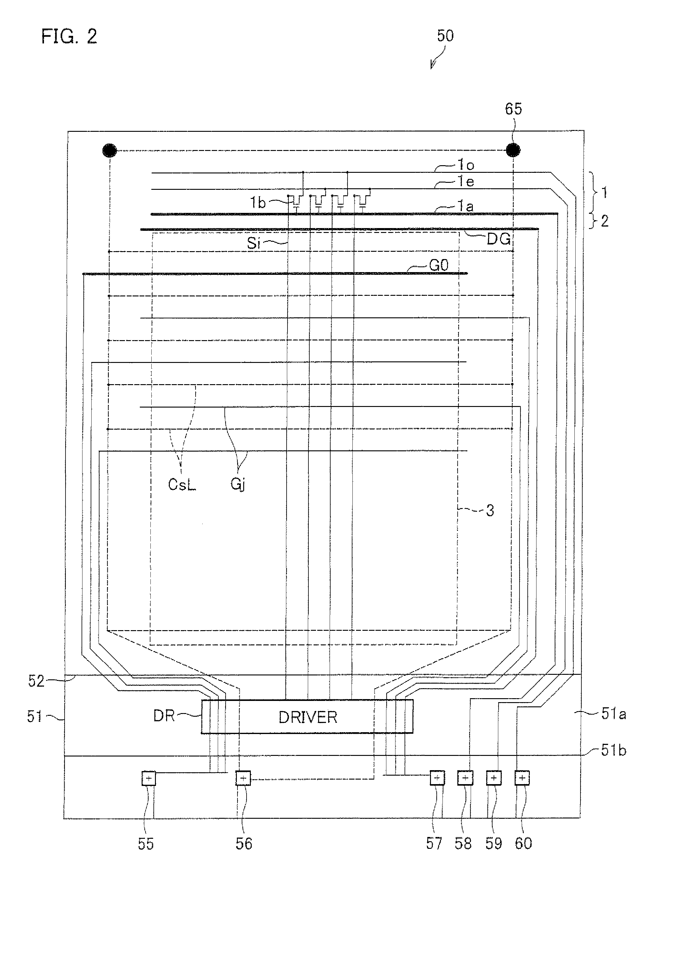
[0079]One embodiment of the present invention is explained below with reference to FIGS. 1, 2, and 8.
[0080]FIG. 1 illustrates a circuit configuration around a boundary between a frame area (peripheral area) and an effective display region, in an active matrix liquid crystal display panel (display panel) according to the present embodiment.
[0081]In the liquid crystal display panel, a test wiring region 1, a dummy pixel region 2, and an effective display region 2 are placed in this order in a direction in which data lines extend. The test wiring region 1 and the dummy pixel region 2 are placed in the frame area and light-shielded by a counter substrate.
[0082]The effective display region 3 is usable for providing view images and arranged such that pixels are respectively provided in regions surrounded by scanning liens GJ (j is an integer) and data lines Si (i is integer) that are provided perpendicularly to each other. An exemplary configuration of the pixels is the same as the one il...
embodiment 2
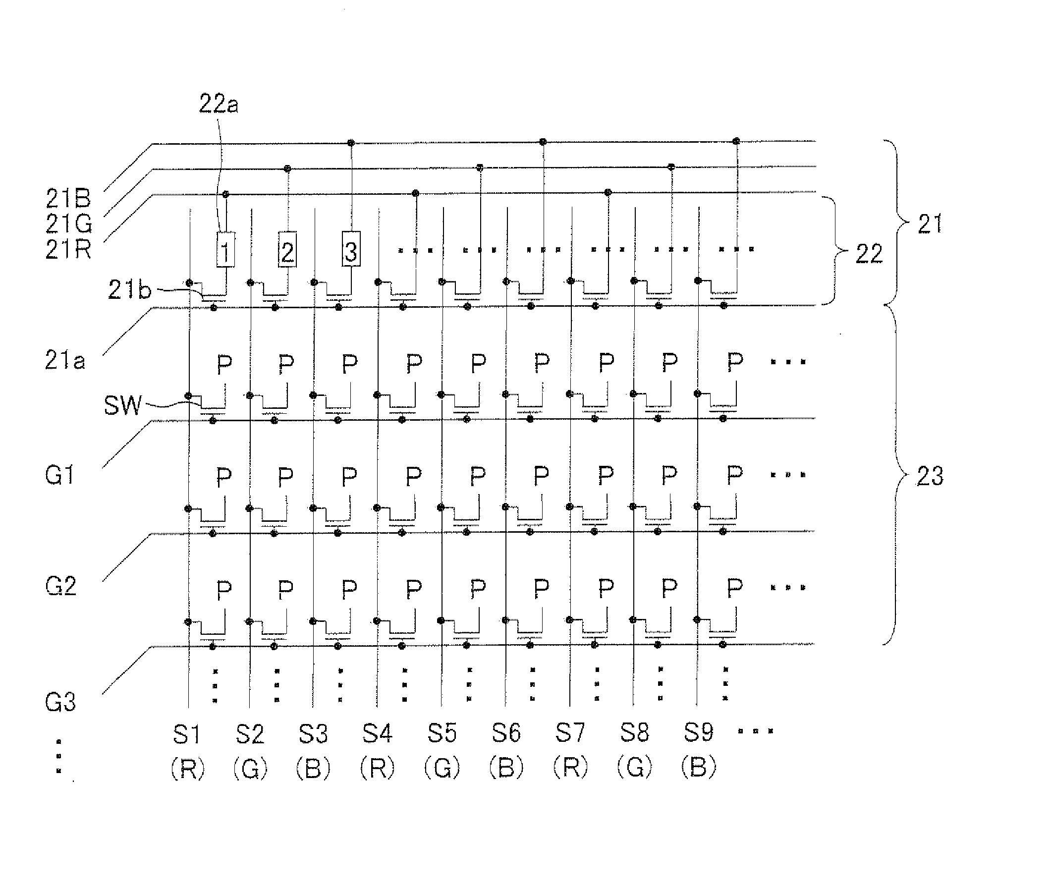
[0103]Another embodiment of the present invention is explained below with reference to FIGS. 3, 4, and 8.
[0104]FIG. 3 illustrates a circuit configuration around a boundary between a frame area and an effective display region, in an active matrix liquid crystal display panel (a display panel) of the present embodiment.
[0105]In the liquid crystal display panel, a test wiring region 21 and an effective display region 23 are placed in this order in a direction in which data lines extend. A part of the test wiring region 21, close to the effective display region, is a dummy pixel region 22. The test wiring region 21 is placed in the frame area and light-shielded by a counter substrate.
[0106]The effective display region 23 is usable for providing view images, and arranged such that pixels are respectively provided in regions surrounded by scanning lines Gj (j is an integer) and data lines Si (i is an integer) that are provided perpendicularly to each other. An exemplary configuration of t...
embodiment 3
[0126]Further another embodiment of the present invention is explained below with reference to FIGS. 5 and 8.
[0127]FIG. 5 illustrates a circuit configuration around a boundary between a frame area and an effective display region, in an active matrix liquid crystal display panel (a display panel) of the present embodiment.
[0128]In the liquid crystal display panel, a test wiring region 31, a dummy pixel region 32, and an effective display region 33 are provided in this order in a direction in which data lines extend. Further, a dummy pixel region 34 is provided on a left of the effective display region 33 and a dummy pixel region 35 is provided on a right thereof, each in a direction in which scanning lines extends. A test wiring region 36 is provided further outside the dummy pixel region 35 in the scanning line direction. The test wiring region 31, the dummy pixel region 2, the dummy pixel region 34, the dummy pixel region 35, and the test wiring region 36 are provided in the frame ...
PUM
 Abstract
Description
Claims
Application Information