Power splitter/ combiner circuit, high power amplifier and balun circuit

a technology of combiner circuit and splitter, which is applied in the direction of phase-splitters, one-port networks, waveguide type devices, etc., can solve the problems of unbalanced power splitting, low versatility of configuration, and large load loss of splitter/combiner

Inactive Publication Date: 2001-03-13
PANASONIC CORP
View PDF5 Cites 43 Cited by
  • Summary
  • Abstract
  • Description
  • Claims
  • Application Information

AI Technical Summary

Problems solved by technology

The configuration shown in FIG. 12B, however, loads to large loss in splitter/combiner due to a long transmission path.
In addition, the configuration also has a problem of low versatility, because power can be split and propagated only to 2.sup.n paths.
Furthermore, the configuration show

Method used


Image

  • Power splitter/ combiner circuit, high power amplifier and balun circuit
  • Power splitter/ combiner circuit, high power amplifier and balun circuit
  • Power splitter/ combiner circuit, high power amplifier and balun circuit

Examples


first embodiment

(First embodiment)

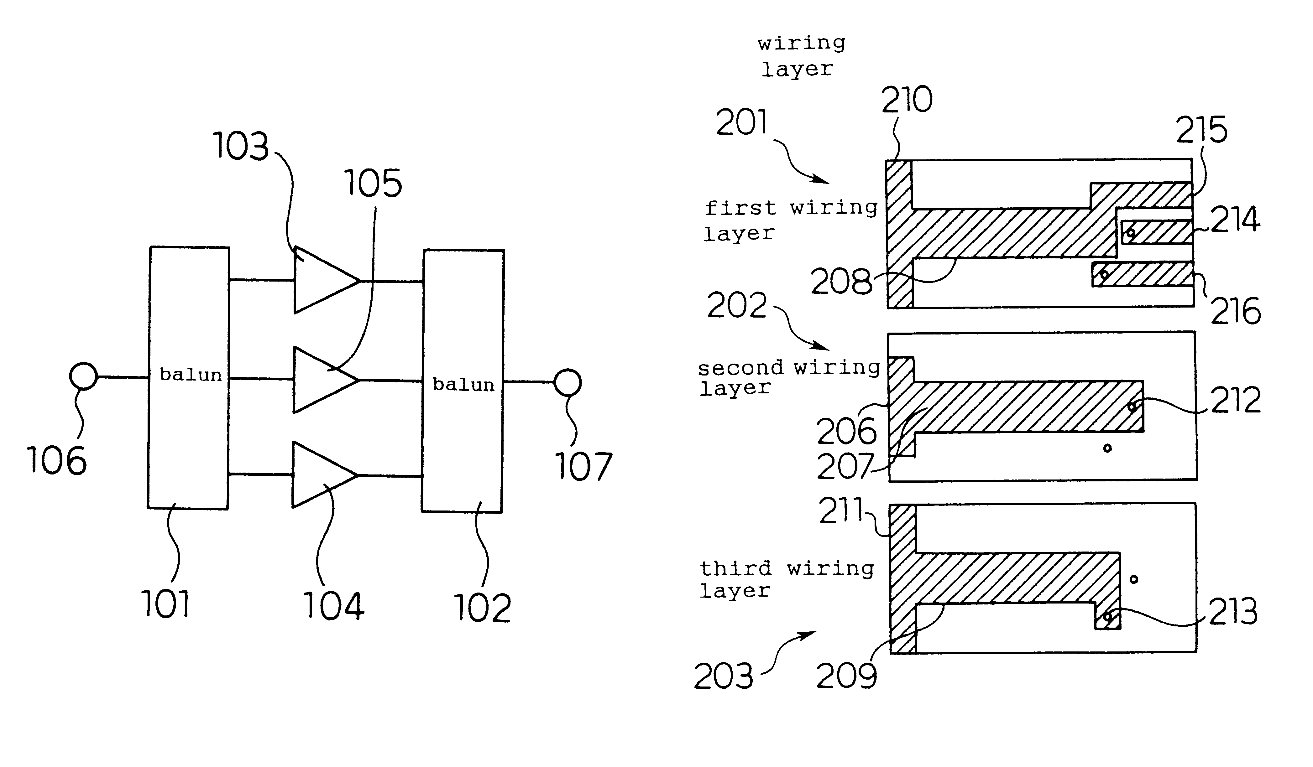
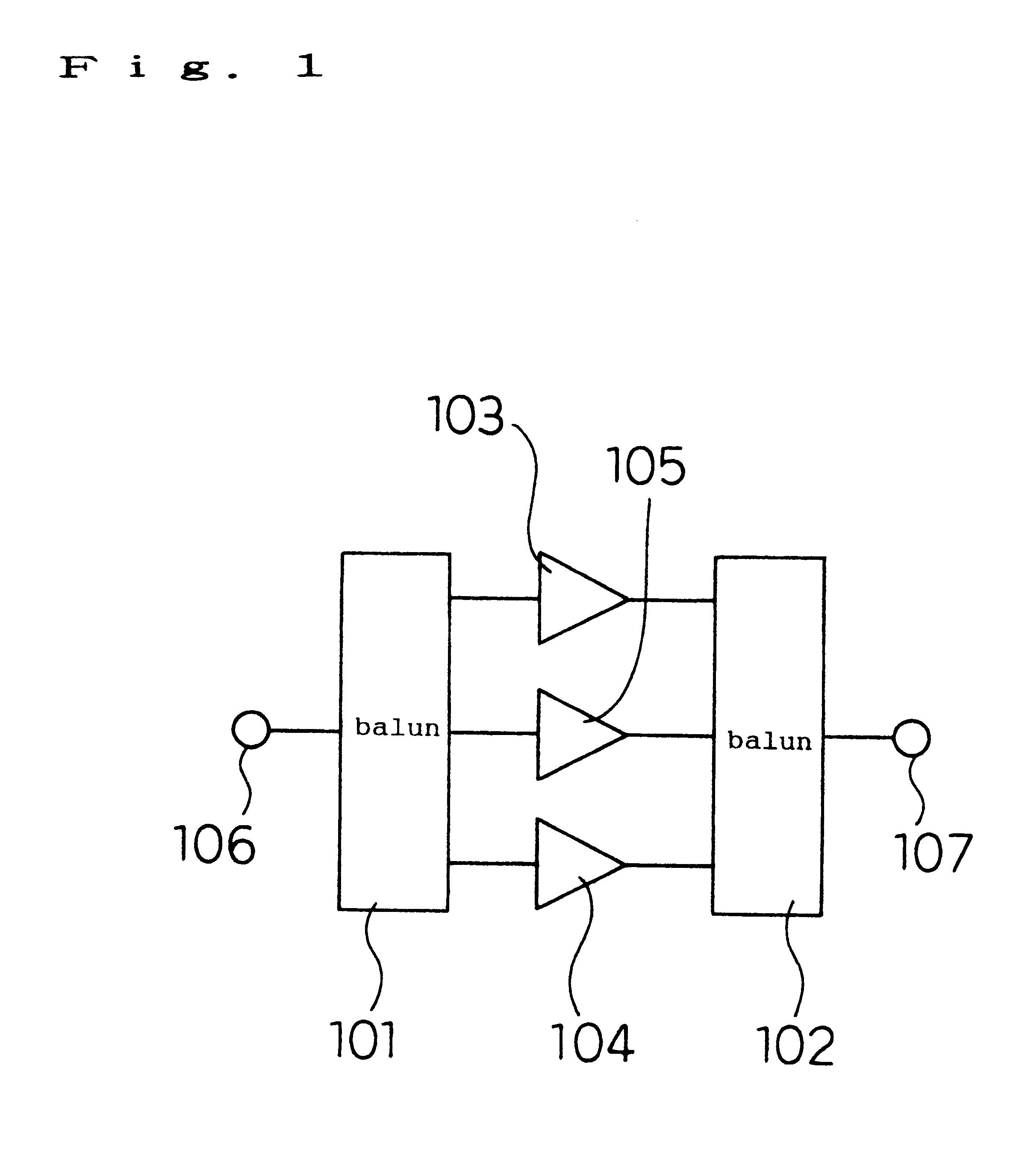
FIG. 1 is a view showing the configuration of a high power amplifier in accordance with a first embodiment of the present invention. Referring to FIG. 1, the numerals 101, 102 designate baluns, the numerals 103, 104 designate power amplifiers having identical characteristics, the numeral 105 designates a power amplifier generating output power twice as high as that of the power amplifier 103 or 104, the numeral 106 designates an input terminal, and the numeral 107 designates an output terminal.

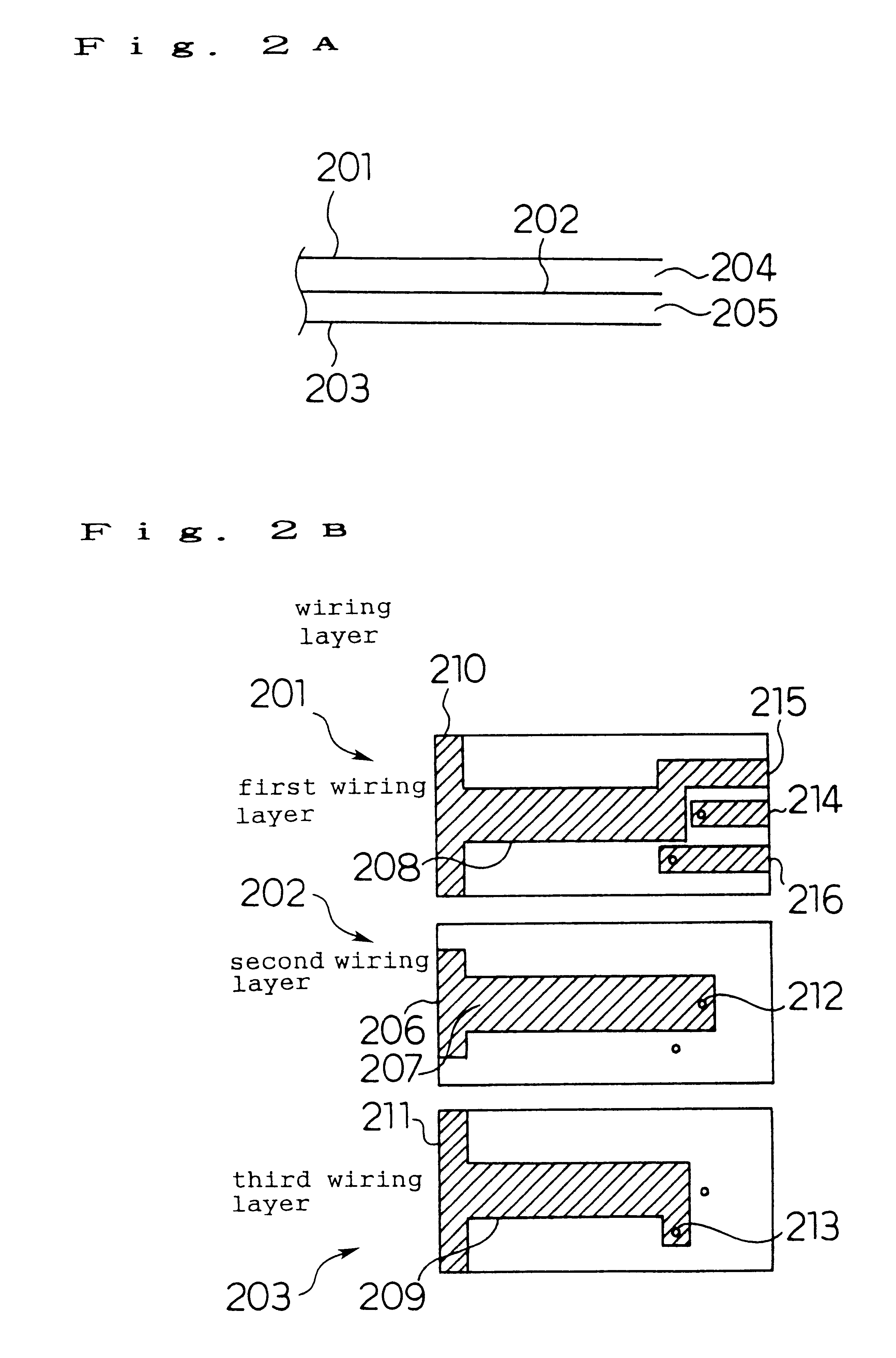
In this configuration, a balun used for the present invention will be detailed below referring to FIGS. 2A to 2C. FIG. 2A is a sectional view showing a balun formed of a dielectric multilayer board, FIG. 2B is a view showing conductor patterns on each conductor pattern layer, and FIG. 2C is a view illustrating the operation of the balun.

Referring to FIG. 2A, the numerals 201, 202, 203 designate first to third conductor pattern layers, and the numerals 204, 205 designate first...

second embodiment

(Second embodiment)

FIG. 3 is a view showing the configuration of a high power amplifier in accordance with a second embodiment of the present invention. Referring to FIG. 3, the numerals 301, 302 designate four-way power splitters, the numeral 303 designates the high power amplifier described in the explanation of the first embodiment, the numeral 304 designates an input terminal, and the numeral 305 designates an output terminal.

In this configuration, the four-way power splitter used for the present invention will be detailed below referring to FIGS. 4A to 4C. FIG. 4A is a sectional view showing the four-way power splitter formed of a dielectric multilayer board. FIG. 4B is a view showing the conductor patterns on the conductor pattern layers of the board. FIG. 4C is a circuit diagram of the four-way splitter. Referring to FIG. 4A, the numerals 401, 402, 403 designate first to third conductor pattern layers, and the numerals 404, 405 designate the first and second dielectric layers...

third embodiment

(Third embodiment)

FIG. 6 is a view showing the configuration of a balun in accordance with a third embodiment of the present invention. Referring to FIG. 6, the numerals 1010, 1020 designate first and second dielectric layers, the numeral 1030 designates an input line, the numeral 1040 designates a main line, the numeral 1050, 1060 designate first and second coupling lines, the numerals 1070, 1080 designate first and second output line pairs, the numerals 1090, 1100 designate first and second through holes, and the numerals 1110, 1120, 1130 designate first to third grounding conductors. It is supposed that the first to third grounding conductors 1110, 1120, 1130 have been electrically connected to one another via through holes or the like (not shown). Among the above-mentioned electrodes and lines, the electrodes and lines disposed on the same plane form each of layers, and these layers correspond to the conductor pattern layers in accordance with the present invention. These conduc...


PUM


Abstract

A high power amplifier has a first balun propagating a half of an input signal to an in-phase output terminal, and also propagating a fourth of the input signal to first and second opposite-phase output terminals, the signal propagated to the first and second opposite-phase output terminals lagging 180 degrees behind the signal propagated to the in-phase output terminal; first and second power amplifier circuits connected to the first and second opposite-phase output terminals of the first balun and having the same characteristics; a third power amplifier circuit connected to the in-phase output terminal of the first balun and having output power substantially twice as much as the output power of the first or second power amplifier circuit; and a second balun having first and second opposite-phase input terminals for receiving the outputs of the first and second power amplifier circuits, having an in-phase input terminal for receiving the output of the third power amplifier circuit, combining the outputs of the first, second and third power amplifier circuits, and propagating combined output.

Description

1. Field of the InventionThe present invention relates to a high power amplifier mainly used at a cellular phone base station, and a balun circuit for the high power amplifier.2. Related Art of the InventionA high power amplifier capable of propagating several tens of watts to several hundreds of watts has recently been used at a digital mobile communication base station. This kind of high power amplifier comprises a plurality of push-pull amplifiers combined in parallel to obtain high power, wherein each push-pull amplifier comprises two same transistors connected in parallel and supplied with signals 180 degrees out of phase with each other. The explanation of the push-pull amplifier has been given on pages 113 to 116 of "Radio Frequency Transistors" written by Norm Dye and Helge Granberg, published by Butterworth / Heinemann. Therefore, no detailed explanation is given here. This power amplifier circuit requires a power splitter / combiner circuit and baluns at each of the input and ...

Claims


Application Information

Patent Timeline
IPC IPC(8): H01P5/12H01P5/10H03F3/60
CPCH01P5/10H01P5/12H03F3/602
Inventor ISHIDA, KAORUMIYAJI, MASAYUKIKOSUGI, HIROAKIKUGOU, SHIN'ICHI
Owner PANASONIC CORP
Why Eureka
Try Eureka