Drive circuit for display apparatus and display apparatus

Inactive Publication Date: 2005-09-22
RENESAS ELECTRONICS CORP
View PDF17 Cites 44 Cited by
  • Summary
  • Abstract
  • Description
  • Claims
  • Application Information

AI Technical Summary

Benefits of technology

[0018] According to another aspect of the invention, there is provided a drive circuit for a display apparatus D/A converting an digital picture to provide an analog picture signal to a data line of the display apparatus. The drive circuit comprises a positive polarity drive circuit outputting the positive polarity analog picture signal with respect to system ground voltage, a negative polarity drive circuit outputting t

Problems solved by technology

It has now been discovered that, however, this conventional drive circuit has several drawbacks.
The second drawback is the large power consumption.
If the com voltage is 5V, the high level voltage of about 10 V of positive polarity is generated in the power source circuit, as a result, the efficiency of the power source circuit decreases and power c

Method used


Image

  • Drive circuit for display apparatus and display apparatus
  • Drive circuit for display apparatus and display apparatus
  • Drive circuit for display apparatus and display apparatus

Examples


embodiment 1

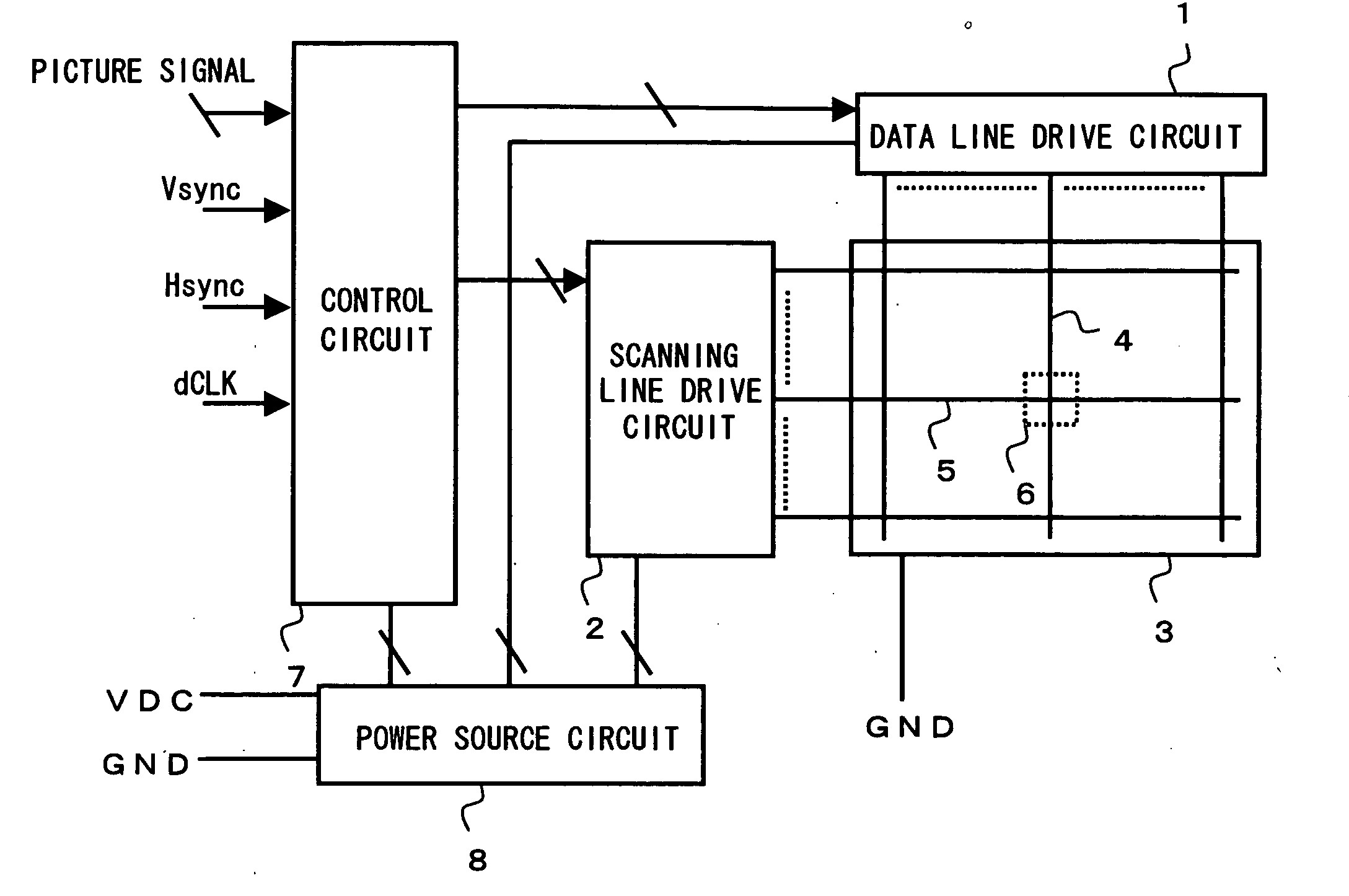
[0068]FIG. 7 is a block diagram of the liquid crystal display of the present embodiment. A plurality of data lines 4 and a plurality of scanning lines 5 arranged perpendicularly to the data lines 4-are formed on a liquid-crystal panel 3, and TFT (Thin Film Transistors) as switching elements and pixels 6 containing liquid crystals and the like are formed at the intersection points of the lines. A common electrode and a display electrode for applying an electric field to the liquid crystal are formed in a pixel.

[0069] An analog picture signal for controlling the brightness (quantity of transmitted light) of the pixel is supplied from the data line to the display electrode, and a com voltage (DC voltage) is supplied to the common electrode. Furthermore, the liquid crystal display comprises a data line drive circuit 1 for driving the data lines 4, a scanning line drive circuit 2 for driving the scanning lines 5, a control circuit 7 for controlling the data line drive circuit 1 and scan...

embodiment 2

[0114] In Embodiment 1, the signal generated by the signal processing circuit 31 is inputted into the positive polarity drive circuit 10 and negative polarity drive circuit 20 via the level shift circuit 32, however, because the inputted signal is a level-shifted voltage, the consumption of power in the picture signal bus is increased. However, as shown in FIG. 29, the increase in power consumption in the picture signal bus can be inhibited by providing a data inversion circuit 315 between the picture signal switching circuit 314 and level shift circuit 32.

[0115] The data inversion circuit 315 comprises a circuit for latching and comparing previous data with next data for each picture signal, a circuit for inverting the picture signal according to the comparison results, and a circuit for generating a video inverted signal INV. The data inversion circuit 315, according to the majority operation, compares the previous data and data subsequent thereto and sets the image inverted sign...

embodiment 3

[0119]FIG. 30 shows a negative polarity level shift circuit different from the negative polarity level shift circuit 322 explained in Embodiment 1. The negative polarity level shift circuit 322 is fabricated from high-voltage elements, however, the negative polarity level shift circuit 324 is fabricated from medium-voltage elements, except the second-stage P channel transistor. The difference between the negative polarity level shift circuits 322 and 324 is in that the low level voltage of the first-stage level shift circuit is VLS (−1×VDC1) (refer to FIG. 31) and the output of the first stage is inputted into the P channel transistor of the second-stage level shift circuit. Furthermore, referring to FIG. 32, an inverter operating at a voltage of VLS-GND may be inserted between the level shift circuit of the first stage and the level shift circuit of the second stage to fabricate all the elements of the level shift circuit with medium-voltage elements.

[0120] With such a circuitry, ...


PUM


Abstract

A drive circuit that is an example of the present invention is a drive circuit of a display device for outputting in parallel the analog picture signals generated based on the digital picture signals inputted in serial. This circuit comprises a level shift circuit for converting the voltage level of the digital picture signals that were inputted in serial, a D/A conversion circuit for generating analog picture signals based on the digital picture signals that were subjected to level conversion with the level shift circuit, and an expansion circuit connected to the output side of the D/A conversion circuit or between the level shift circuit and the D/A conversion circuit and serving to expand and hold the inputted serial picture signals in parallel and output the picture signals in parallel. The level shift circuit is thus formed in the front stage of the picture signal register circuit.

Description

BACKGROUND OF THE INVENTION [0001] 1. Field of the Invention [0002] The present invention relates to a drive circuit of a display device and to a display device, and more particularly to a drive circuit suitable for liquid crystal display devices with a dot inversion drive. [0003] 2. Description of the Related Art [0004] Liquid crystal displays are employed as displays for various lightweight and thin electronic devices with low power consumption, such as cellular phones. As liquid crystal displays, a simple matrix type and an active matrix type (AMLCD: Active Matrix Liquid crystal display) using active elements such as TFTs (Thin Film Transistors) in a pixel circuit are known. [0005]FIG. 1 is a block diagram of a well-known liquid crystal display. The liquid crystal display comprises a scanning line drive circuit 2, a liquid-crystal panel 3, a control circuit 7, a data line drive circuit 51, a power source circuit 58, and a common voltage generation circuit 59. Picture signals, ver...

Claims


Application Information

Patent Timeline
IPC IPC(8): G02F1/133G09G3/20G09G3/36
CPCG09G3/3607G09G3/3614G09G3/3648G09G3/3655G09G3/3688G09G2330/021G09G2310/027G09G2310/0289G09G2310/0297G09G2310/06G09G2320/0219G09G2310/0248A61H23/006A61H23/0254A61H2201/0165A61H2201/1418A61H2201/149A61H2201/50A61H2205/12
Inventor HASHIMOTO, YOSHIHARU
Owner RENESAS ELECTRONICS CORP
Why Eureka
Try Eureka