Semiconductor light-emitting device, lighting module, lighting device and method for manufacturing semiconductor light-emitting device

a technology of semiconductor light-emitting devices and semiconductors, which is applied in the direction of semiconductor/solid-state device manufacturing, semiconductor devices, electrical devices, etc., can solve the problems of insufficient luminous flux of light obtained from the module, difficulty in improving the yield, and difficulty in densely mounting white leds, etc., to achieve less color uniformity and high luminous flux

Active Publication Date: 2008-09-02
PANASONIC CORP
View PDF22 Cites 125 Cited by
  • Summary
  • Abstract
  • Description
  • Claims
  • Application Information

AI Technical Summary

Problems solved by technology

The module proposed by JP 2003-124528 A, however, has the following problem: since a large number of white LEDs are flip-chip mounted on the mounting board, a failure in mounting of one white LED directly leads to a defective module, thus making it difficult to improve the yield.
The module proposed by JP 2001-15817 A, however, has a difficulty in densely mounting the white LEDs.
Therefore, there is a possibility of a shortage in luminous flux of the light obtained from the module.
Further, since the phosphor layer is formed in a substantially rectangular parallelepiped shape, the light extracted from the module has anisotropy, and therefore the extracted light may have non-uniformity in color.

Method used


Image

  • Semiconductor light-emitting device, lighting module, lighting device and method for manufacturing semiconductor light-emitting device
  • Semiconductor light-emitting device, lighting module, lighting device and method for manufacturing semiconductor light-emitting device
  • Semiconductor light-emitting device, lighting module, lighting device and method for manufacturing semiconductor light-emitting device

Examples


embodiment 1

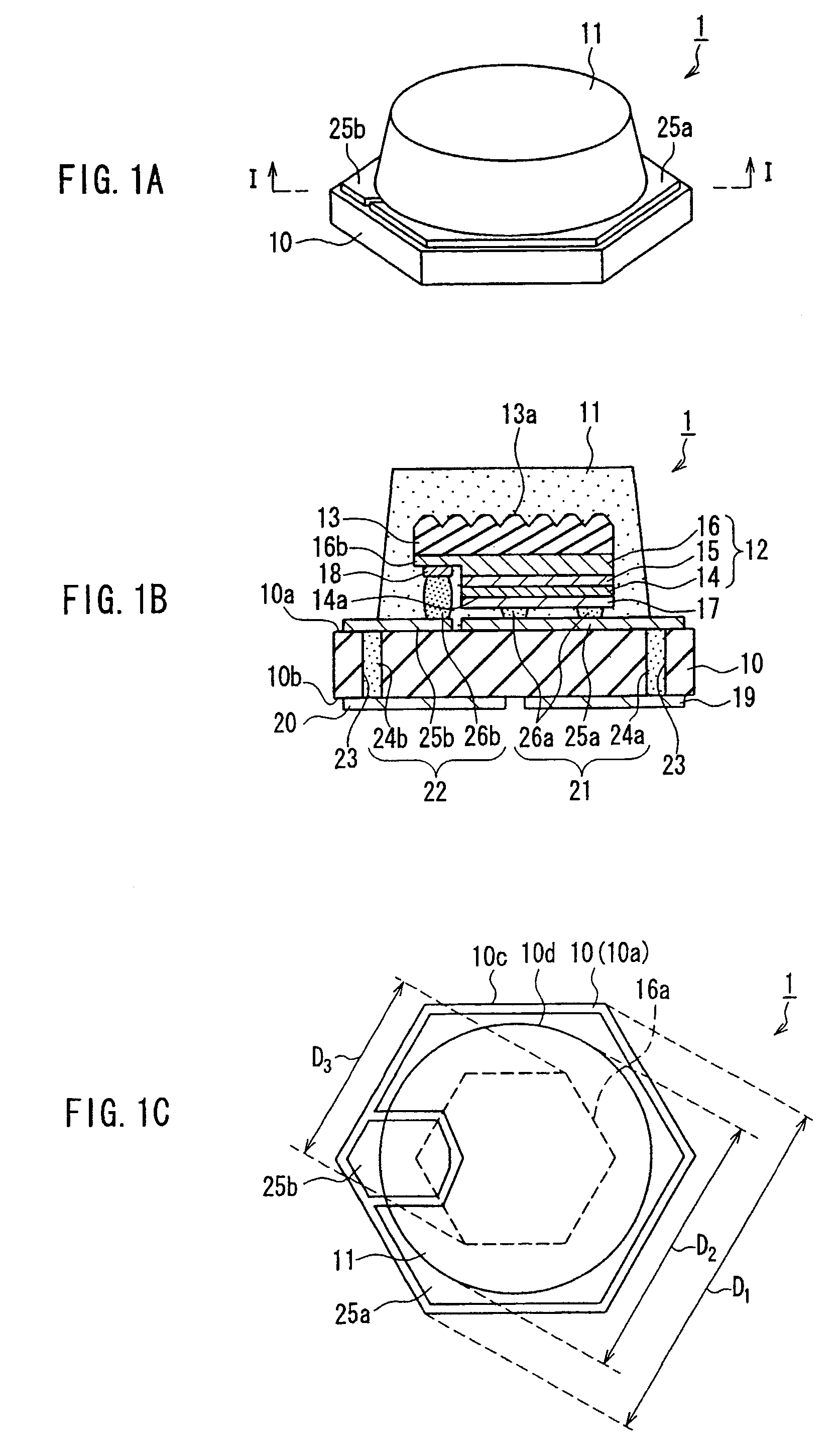
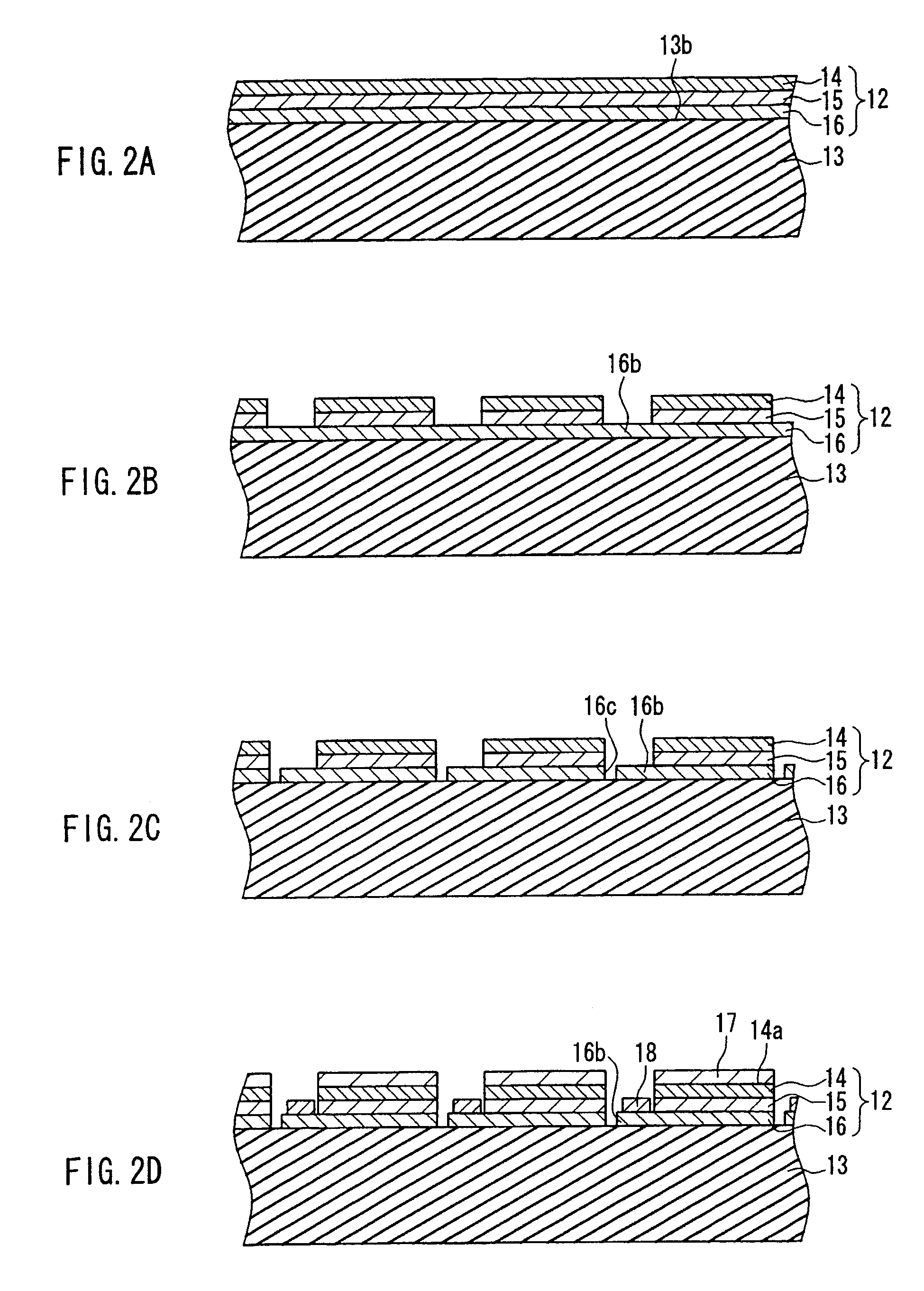
[0087]Firstly, a semiconductor light-emitting device according to Embodiment 1 of the present invention will be described with reference to the drawings. FIG. 1 to be referred to herein is for explaining the semiconductor light-emitting device according to Embodiment 1, where FIG. 1A is a perspective view of the semiconductor light-emitting device according to Embodiment 1, FIG. 1B is a cross-sectional view taken along the line I-I of FIG. 1A and FIG. 1C is a schematic plan view of the semiconductor light-emitting device according to Embodiment 1 when viewing from its phosphor layer side.

[0088]The semiconductor light-emitting device 1 according to Embodiment 1, as shown in FIGS. 1A and B, includes: an electrical insulating substrate 10 formed in a substantially regular hexagonal prism shape; a phosphor layer 11 provided on the electrical insulating substrate 10 and formed in a substantially truncated cone shape; a semiconductor multilayer film 12 provided on the electrical insulatin...

embodiment 2

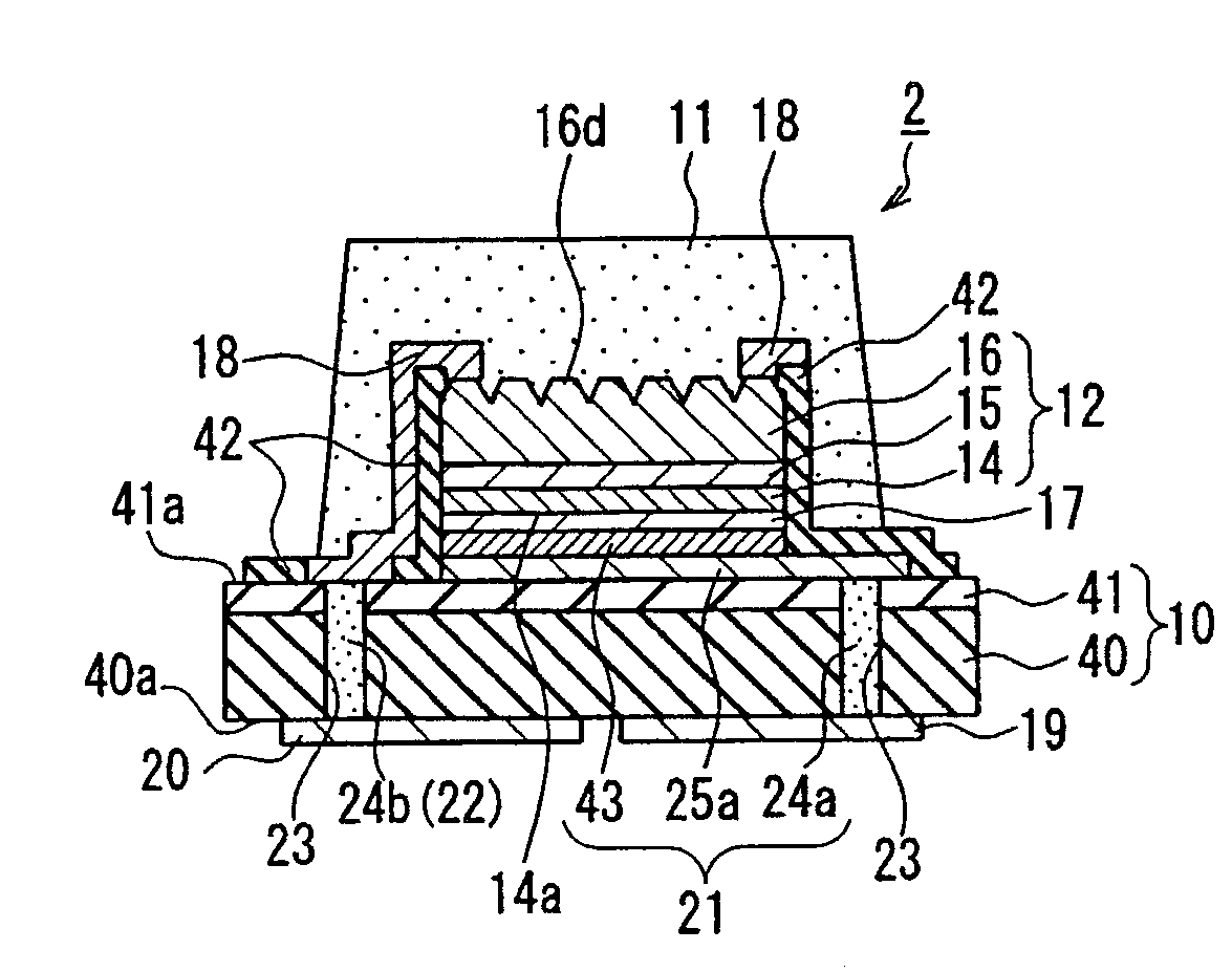
[0112]The following describes a semiconductor light-emitting device according to Embodiment 2 of the present invention, with reference to the drawings. FIG. 8 to be referred to herein is for explaining a semiconductor light-emitting device according to Embodiment 2, where FIG. 8A is a cross-sectional view of the semiconductor light-emitting device according to Embodiment 2, and FIG. 8B is a schematic plan view of the semiconductor light-emitting device according to Embodiment 2 when viewing from its phosphor layer side. Note here that the same reference numerals are assigned to the same elements as those in FIGS. 1A to C and their explanations are omitted.

[0113]The semiconductor light-emitting device 2 according to Embodiment 2, as shown in FIGS. 8A and B, includes: an electrical insulating substrate 10 formed in a substantially regular hexagonal prism shape; a phosphor layer 11 provided on the electrical insulating substrate 10 and formed in a substantially truncated cone shape; an...

embodiment 3

[0137]The following describes a semiconductor light-emitting device according to Embodiment 3 of the present invention, with reference to the drawings. FIG. 15 to be referred to herein is for explaining a semiconductor light-emitting device according to Embodiment 3, where FIG. 15A is a cross-sectional view of the semiconductor light-emitting device according to Embodiment 3, and FIG. 15B is a schematic plan view of the semiconductor light-emitting device according to Embodiment 3 when viewing from its phosphor layer side. Note here that the same reference numerals are assigned to the same elements as those in FIGS. 1A to C and FIGS. 8A and B and their explanations are omitted.

[0138]The semiconductor light-emitting device 3 according to Embodiment 3, as shown in FIGS. 15A and B, includes: an electrical insulating substrate 10 formed in a substantially regular hexagonal prism shape; a phosphor layer 11 provided on the electrical insulating substrate 10 and formed in a substantially t...


PUM


Abstract

A semiconductor light-emitting device includes: a semiconductor multilayer film, a substrate supporting the semiconductor multilayer film; and a phosphor layer formed on the substrate so as to cover the semiconductor multilayer film. The phosphor layer has an outer edge of a cross section taken in a direction parallel to the principal surface of the substrate having a substantially circular shape or a substantially regular polygonal shape having five or more sides. An outer edge of the principal surface of the substrate is formed in a substantially circular shape or a substantially regular polygonal shape having five or more sides. With this configuration, light obtained therefrom has less non-uniformity in color and a high luminous flux can be realized.

Description

TECHNICAL FIELD[0001]The present invention relates to a semiconductor light-emitting device and a lighting module and a lighting device using the same, and also relates to a method for manufacturing a semiconductor light-emitting device.BACKGROUND ART[0002]In general, a GaN-based light-emitting diode (hereinafter abbreviated as “LED”) is composed of a semiconductor multilayer film obtained by crystal-growing a III-V group nitride semiconductor, represented by the general formula BzAlxGa1-x-y-zInyN1-v-wAsvPw (0≦x≦1, 0≦y≦1, 0≦z≦1, 0≦x+y+z≦1, 0≦v≦1, 0≦w≦1, 0≦v+w≦1), on a single crystal substrate such as a sapphire substrate. By feeding a current through this semiconductor multilayer film, wide range of light from an ultraviolet region to an infrared region (e.g., 200 to 1700 nm) can be emitted therefrom. Especially, a LED emitting light in a wavelength region shorter than a blue-green region currently is developed eagerly.[0003]Above all, a blue LED emitting blue light can be combined ...

Claims


Application Information

Patent Timeline
Patent Type & Authority Patents(United States)
IPC IPC(8): H01L33/00H01L33/32H01L33/36H01L33/50H01L33/56H01L33/58H01L33/60H01L33/62
CPCH01L33/22H01L33/505H01L33/56H01L24/24H01L24/97H01L33/20H01L33/44H01L33/486H01L33/62H01L2924/12041H01L2933/0091H01L2224/16225H01L2924/00H01L33/385H01L2924/12042H01L2224/05573H01L2224/05568H01L2224/05624H01L2224/05666H01L2224/05669H01L2924/00014H01L2224/0554H01L2224/05599H01L2224/0555H01L2224/0556
Inventor NAGAI, HIDEO
Owner PANASONIC CORP
Why Eureka
Try Eureka