
Zone control heater plate for track lithography systems

a technology of lithography system and heater plate, which is applied in the direction of hot plate heating arrangement, ohmic resistance heating, electrical equipment, etc., can solve the problems of large number of wires and challenges, and achieve high controllability, effective and efficient solution, and high controllability

Inactive Publication Date: 2008-09-23
SOKUDO CO LTD
View PDF18 Cites 5 Cited by
  • Summary
  • Abstract
  • Description
  • Claims
  • Application Information

AI Technical Summary

Benefits of technology

This design enables highly controllable and efficient heating of substrates, reducing thermal non-uniformities and improving process uniformity in semiconductor manufacturing by effectively managing the large number of wires and maintaining precise temperature control across independently controllable zones.

Problems solved by technology

Effectively and efficiently managing such a large number of wires presents challenges.

Method used


Image

  • Zone control heater plate for track lithography systems
  • Zone control heater plate for track lithography systems
  • Zone control heater plate for track lithography systems

Examples


Embodiment Construction

[0016]The present invention generally provides a method and apparatus for heating substrates in a highly controllable manner. While it is to be recognized that embodiments of the invention are particularly useful for heating substrates according a particular thermal recipe within a track lithography tool, other embodiments of the invention can be used in other applications where it is desirable to heat substrates in a highly controllable manner. Note the terms “substrate” and “wafer” are sometimes used herein interchangeably and are sometimes specifically used in reference to a semiconductor wafer upon which integrated circuits are formed. A person of skill in the art will recognize the present invention is not limited to processing semiconductor wafers and can be used to process any substrate for which a highly controlled thermal treatment is desirable.

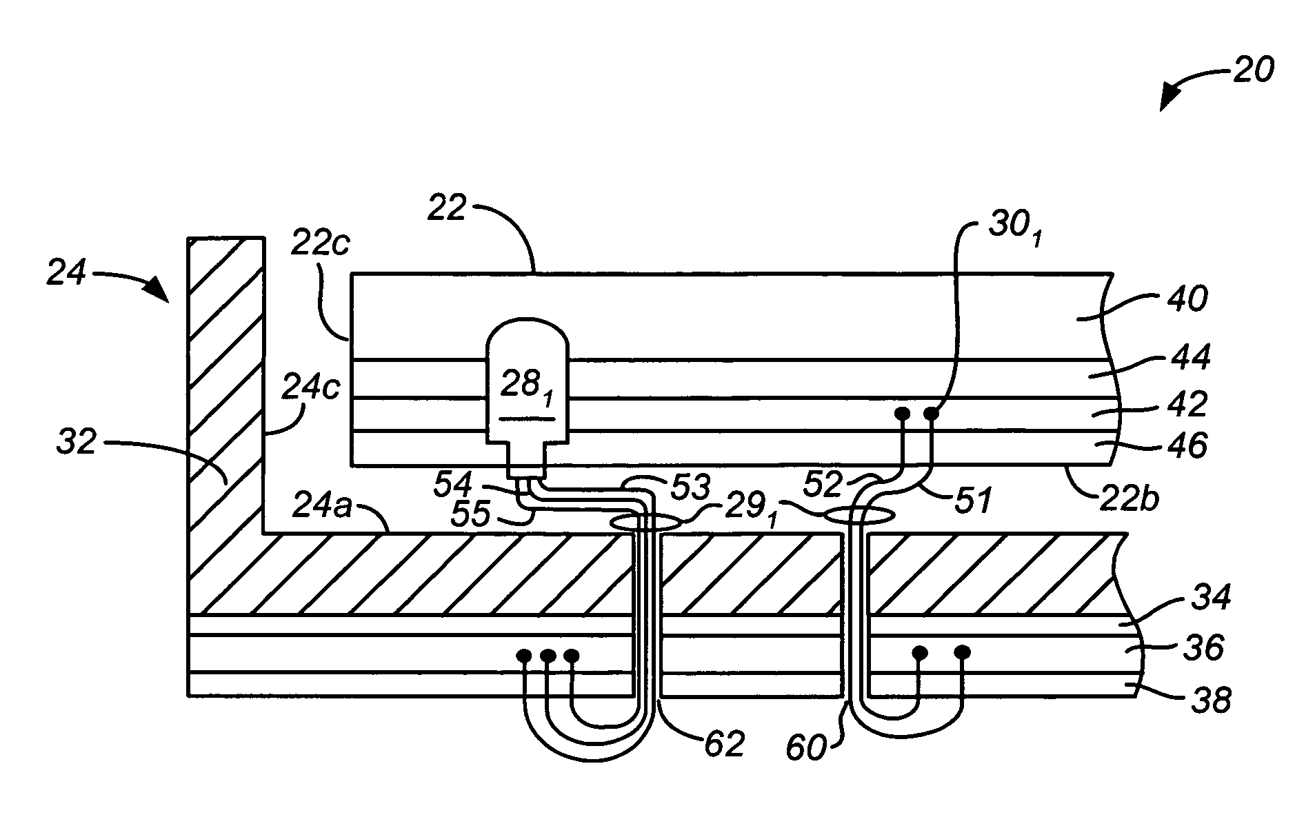
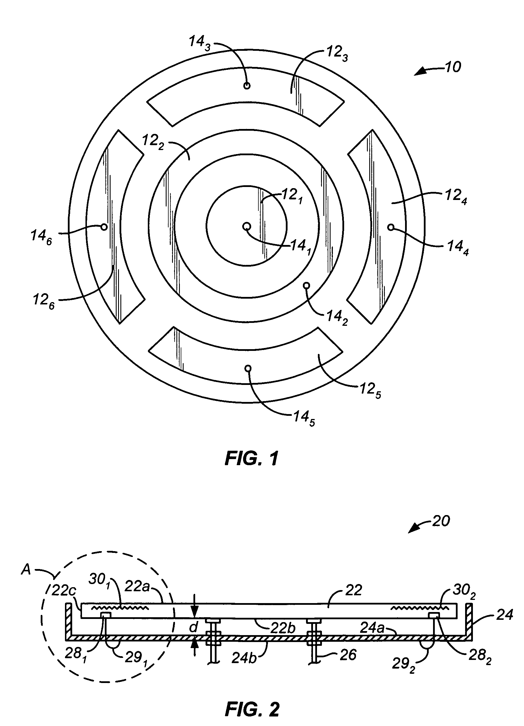
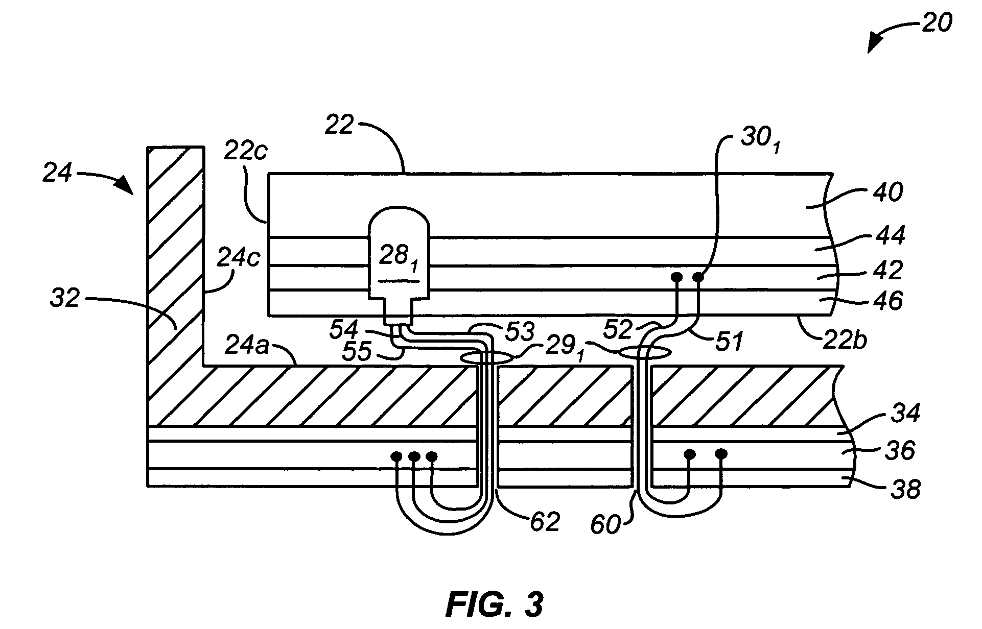
[0017]Reference is now made to FIG. 2, which is a simplified cross-sectional view of a substrate heater 20 according to an embodime...


PUM


Abstract

A substrate heater comprising a bake plate having an upper surface, a lower surface and a peripheral side surface extending between the upper and lower surfaces, the bake plate including at least one heating element, at least one temperature sensor and a plurality of wires including at least one wire coupled to the heating element and at least one wire coupled to the temperature sensor; a shield spaced apart from and generally surrounding the lower and peripheral side surfaces of the bake plate, the shield having an interior upper surface facing the lower surface of the bake plate, an interior side surface facing the peripheral side surface of the bake plate and a lower surface opposite the interior upper surface; a patterned signal layer formed on the lower surface of the shield, wherein the plurality of wires are electrically coupled to a corresponding plurality of signal traces formed in the patterned signal layer; and a connector, electrically coupled to the plurality of signal traces in the patterned signal layer, adapted to facilitate electrical connections to the plurality of wires.

Description

BACKGROUND OF THE INVENTION[0001]The present invention relates generally to the field of substrate processing equipment. More particularly, the present invention relates to a method and apparatus for controlling the temperature of substrates, such as semiconductor substrates, used in the formation of integrated circuits.[0002]Modern integrated circuits (ICs) contain millions of individual elements that are formed by patterning the materials, such as silicon, metal and / or dielectric layers, that make up the integrated circuit to sizes that are small fractions of a micrometer. A number of steps associated with the fabrication of integrated circuits include heating the semiconductor substrate upon which the ICs are formed. One example of a heating step includes curing a photoresist film prior to a photolithography process. A photoresist film can be cured, for example, by placing a semiconductor substrate having an uncured photoresist film formed thereon on a bake plate and heating the ...

Claims


Application Information

Patent Timeline
Patent Type & Authority Patents(United States)
IPC IPC(8): H05B3/68
CPCH01L21/67103H05B3/143H01L21/67248
Inventor SALINAS, MARTIN JEFFQUACH, DAVID H.
Owner SOKUDO CO LTD
Learn More