Method of fabricating strain-silicon CMOS

Active Publication Date: 2008-09-30
XILINX INC
View PDF33 Cites 74 Cited by
  • Summary
  • Abstract
  • Description
  • Claims
  • Application Information

AI Technical Summary

Benefits of technology

[0016]Recesses are formed in the drain and source regions of an MOS transistor. The recesses are formed using two anisotropic etch processes and first and second sidewall spacers. The recesses are made up of first and second recesses, and the depths of the first and secon

Problems solved by technology

However, the edges 112 of the SiGe regions are relatively far from the channel region 110, reducing their effectiveness at producing the desired strain in the channel

Method used


Image

  • Method of fabricating strain-silicon CMOS
  • Method of fabricating strain-silicon CMOS
  • Method of fabricating strain-silicon CMOS

Examples


Example

DETAILED DESCRIPTION OF THE DRAWINGS

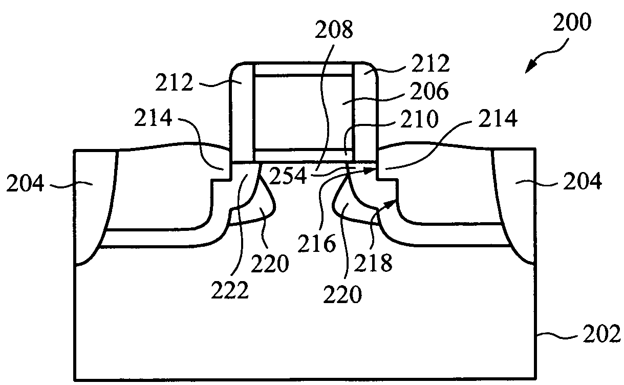
[0024]FIG. 2 is a simplified cross section of an MOS transistor 200 according to an embodiment of the invention. The MOS transistor 200 is fabricated on a substrate 202, such as a silicon wafer or silicon-on-insulator (SOI) wafers. In an IC, many transistors are fabricated on a piece of the substrate, commonly called a die or chip. Transistors on a chip are often separated by trench isolation dielectric 204 or other isolation structure.

[0025]A gate 206 is isolated from a channel region 208 by a gate dielectric layer 210. Sidewall spacers 212 align regions of stressed material 214 to the channel region 208. The stressed material 214 has a first edge 216 close to the channel region 208 and next to a source / drain extension region 254, and a second edge 218 that is further away from the channel region and extends deeper into the substrate 202, both edges along one end of the stressed material. The regions of stressed material 214 induce strain in the ...


PUM


Abstract

Recesses are formed in the drain and source regions of an MOS transistor. The recesses are formed using two anisotropic etch processes and first and second sidewall spacers. The recesses are made up of first and second recesses, and the depths of the first and second recesses are independently controllable. The recesses are filled with a stressed material to induce strain in the channel, thereby improving carrier mobility. The widths and depths of the first and second recesses are selectable to optimize strain in the channel region.

Description

FIELD OF THE INVENTION[0001]The present invention relates generally to semiconductor devices, and more particularly to semiconductor devices having improved mobility due to channel strain.BACKGROUND OF THE INVENTION[0002]Programmable logic devices (PLDs) are a well-known type of integrated circuit that can be programmed to perform specified logic functions. One type of PLD, the field programmable gate array (FPGA), typically includes an array of programmable tiles. These programmable tiles can include, for example, input / output blocks (IOBs), configurable logic blocks (CLBs), dedicated random access memory blocks (BRAM), multipliers, digital signal processing blocks (DSPs), processors, clock managers, delay lock loops (DLLs), transceivers, and so forth.[0003]Each programmable tile typically includes both programmable interconnect and programmable logic. The programmable interconnect typically includes a large number of interconnect lines of varying lengths interconnected by programm...

Claims


Application Information

Patent Timeline
IPC IPC(8): H01L29/76
CPCH01L21/823807H01L21/823814H01L29/7848H01L29/7834H01L29/66636
Inventor NAYAK, DEEPAK KUMARLUO, YUHAO
Owner XILINX INC
Why Eureka
Try Eureka