Circuits to delay a signal from DDR-SDRAM memory device including an automatic phase error correction

a technology of ddr-sdram and memory device, which is applied in the direction of information storage, static storage, digital storage, etc., can solve the problems of increasing the complexity of writing data to and reading data from ddr-sdram devices

Active Publication Date: 2008-10-07
ATMEL CORP
View PDF29 Cites 18 Cited by
  • Summary
  • Abstract
  • Description
  • Claims
  • Application Information

AI Technical Summary

Problems solved by technology

This feature increases the complexity of writing data to and reading data from the DDR-SDRAM device since the valid-data window is narrower than in SDR-SDRAM devices.

Method used


Image

  • Circuits to delay a signal from DDR-SDRAM memory device including an automatic phase error correction
  • Circuits to delay a signal from DDR-SDRAM memory device including an automatic phase error correction
  • Circuits to delay a signal from DDR-SDRAM memory device including an automatic phase error correction

Examples


Embodiment Construction

[0031]Persons of ordinary skill in the art will realize that the following description of the present invention is illustrative only and not in any way limiting. Other embodiments of the invention will readily suggest themselves to such skilled persons.

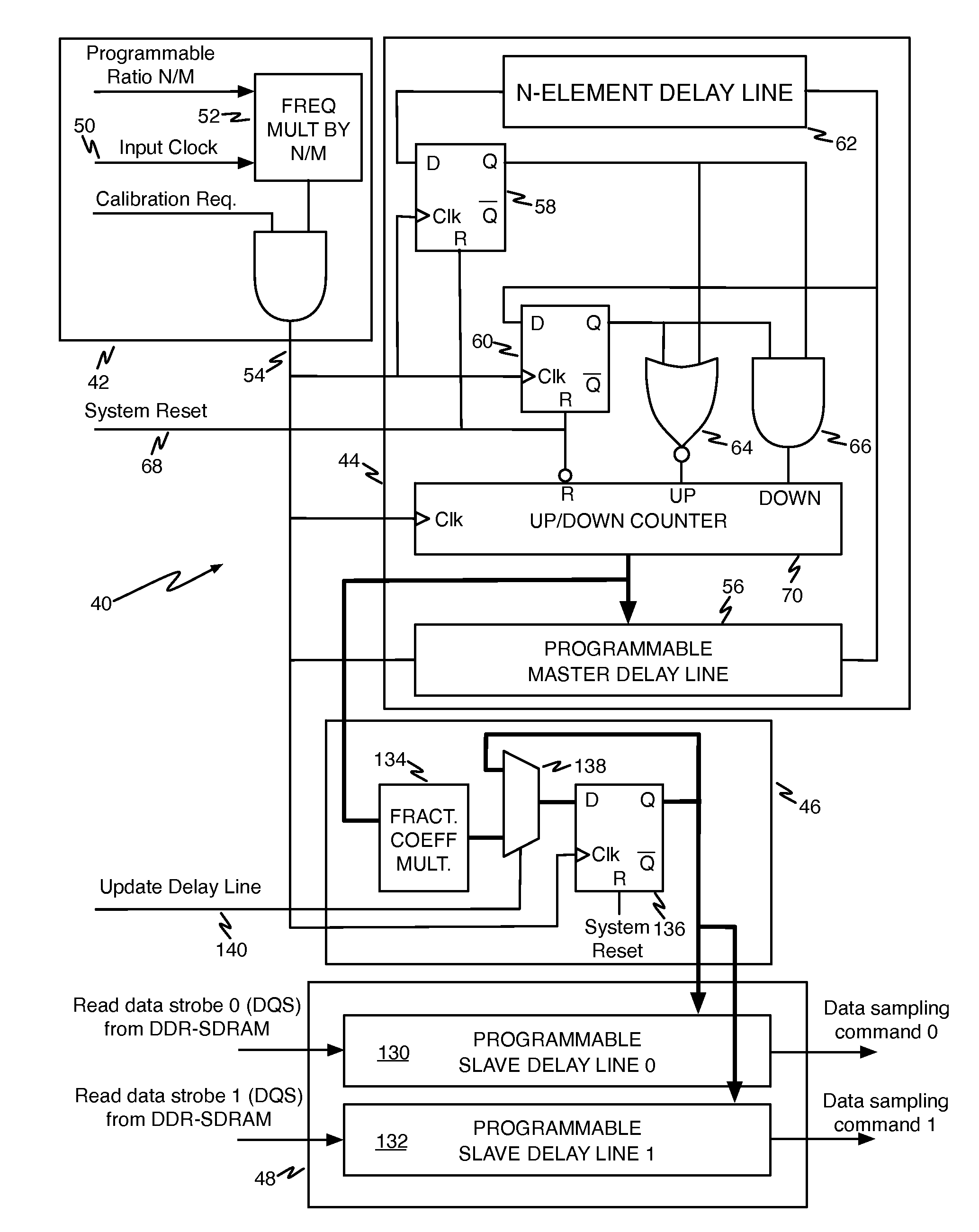
[0032]Referring now to FIG. 4, a block diagram illustrates a typical environment in which the present invention may be employed. FIG. 4 shows a system including a microcontroller 10 connected to a DDR-SDRAM device 12 through a DDR memory controller 14. An input clock signal, shown at reference numeral 16, provides a clock reference signal to DQS delay circuitry 18. The function of DQS delay circuitry 18 is to delay the DQS(0) and DQS(1) signals from DDR-SDRAM device 12 to produce a delayed DQS(0) and a delayed DQS(1) signal to control reading data from DDR-SDRAM device 12. It is to a DQS delay circuitry 18 that the present invention is directed.

[0033]As may be seen from an examination of FIG. 4, the delayed DQS(0) and delayed DQS(1) s...


PUM


Abstract

A method for delaying a control signal, includes receiving a clock signal, determining a number of delay elements required to generate a first delay equal to a target amount of the period of the clock signal, receiving a data signal having an edge generated at the same time as an edge of the control signal, determining a fraction number equal to the number of delay elements needed to generate a second delay for the data signal or the control signal to align their edges, divided by the number of cascaded delay elements necessary to provide a delay equal to the target amount of the period of the clock signal, multiplied by the number of delay elements to generate the first delay, and delaying the control signal by the number of cascaded delay elements to realize said first delay altered by the fraction number of delay elements.

Description

RELATED APPLICATIONS[0001]This application is a continuation-in-part of co-pending application Ser. No. 11 / 466,311, filed Aug. 22, 2006.BACKGROUND OF THE INVENTION[0002]1. Field of the Invention[0003]The present invention relates to dual-data-rate dynamic-random-access-memory (DDR-SDRAM) devices. More particularly, the present invention relates to circuits to delay the “DQS” signal from a DDR-SDRAM memory device to capture data, the “DQS” signal and the data being generated simultaneously by the memory device, the circuits including a fine delay tuning capability.[0004]2. The Prior Art[0005]DDR-SDRAM devices can transfer data twice as fast as single-data-rate SDRAM memory devices (SDR-SDRAM). This is because DDR-SDRAM devices can send and receive signals twice per clock cycle. This feature increases the complexity of writing data to and reading data from the DDR-SDRAM device since the valid-data window is narrower than in SDR-SDRAM devices.[0006]Referring now to FIGS. 1A and 1B, a t...

Claims


Application Information

Patent Timeline
Patent Type & Authority Patents(United States)
IPC IPC(8): G11C8/00
CPCG11C29/02G11C29/023G11C29/028G11C11/401G11C2029/0409
Inventor VERGNES, ALAINMATULIK, ERICSCHUMACHER, FREDERIC
Owner ATMEL CORP
Why Eureka
Try Eureka