

Semiconductor element
a technology of semiconductor elements and elements, applied in the direction of semiconductor devices, semiconductor/solid-state device details, electrical apparatus, etc., can solve the problems of inability to adequately suppress the diffusion of silver into the electrode material, decrease the light emission intensity, and the service life is reduced, so as to prolong the service life and prevent the migration of silver. , the effect of increasing the light emission intensity
- Summary
- Abstract
- Description
- Claims
- Application Information
AI Technical Summary
Benefits of technology
Problems solved by technology
Method used
Image

Examples
working example 1
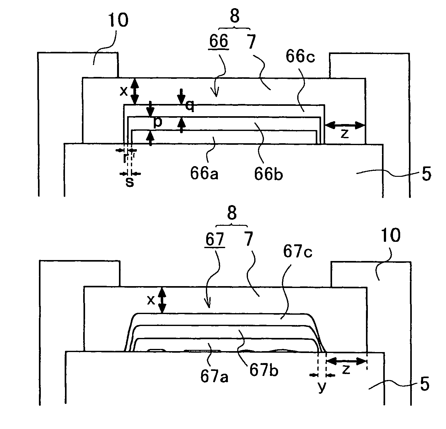
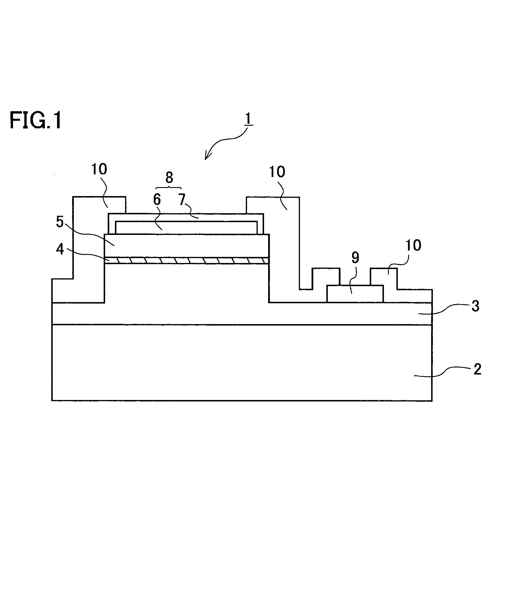
[0226]FIG. 1 illustrates the semiconductor element in this working example.
[0227]This semiconductor element 1 was configured as follows; a buffer layer (not shown) composed of Al0.1Ga0.9N and a non-doped GaN layer (not shown) were formed over a sapphire substrate 2. Over this were formed, as an n-type semiconductor layer 3 an n-type contact layer composed of silicon-doped GaN, and a super-lattice n-type clad layer produced by alternately forming a GaN layer (40 Å) and an InGaN layer (20 Å) for 10 iterations. Over this were formed a light emitting layer 4 with a multiple quantum well structure and produced by alternately forming a GaN layer (250 Å) and an InGaN layer (30 Å) for 3 to 6 iterations, and as a p-type semiconductor layer 5, a super-lattice p-type clad layer produced by alternately forming a magnesium-doped Al0.1Ga0.9N layer (40 Å) and a magnesium-doped InGaN layer (20 Å) for 10 iterations, and a p-type contact layer composed of magnesium-doped GaN, layered in that order.
[0...
working example 2
[0245]The semiconductor element of this working example was constituted the same as the semiconductor element in Working Example 1, except that a multilayer film consisting of an upper layer of platinum, a middle layer of nickel, and a lower layer of silver was formed, in a thickness of 1000 Å, 1000 Å, and 1000 Å, instead of the silver electrode in Working Example 1, and the annealing temperature after the formation of the p-electrode 8 and the n-electrode 9 was raised to about 600° C.
[0246]The semiconductor element obtained as above was connected to power under the same conditions as in Working Example 1, but the ohmic properties were still good and no migration had occurred even after 10,000 hours of continuous powered operation, meaning that a semiconductor element of high quality and reliability had been obtained.
[0247]Furthermore, the silver electrode was checked before and after power was applied, and crystal grains of about 100 nm were observed in a quantity of about 50% over...
working example 3
[0249]The semiconductor element of this working example was constituted the same as the semiconductor element in Working Example 1, except that SiON was used instead of the SiN used in Working Example 2.
[0250]The performance of the semiconductor element thus obtained varied with the operating environment, but when the humidity was relatively low, for instance, the ohmic properties were just as good as in Working Example 2 in every case, and no migration occurred, meaning that a semiconductor element of high quality and reliability had been obtained.
PUM
| Property | Measurement | Unit |
|---|---|---|
| temperature | aaaaa | aaaaa |
| thickness | aaaaa | aaaaa |
| thickness | aaaaa | aaaaa |
Abstract
Description
Claims
Application Information