Semiconductor element

a technology of semiconductor elements and semiconductors, applied in the field of semiconductor elements, can solve the problems of inability to adequately suppress the diffusion of silver into the electrode material, reduce the service life, and reduce so as to prolong the service life, increase the light emission intensity, and prevent the effect of silver migration

Active Publication Date: 2007-02-01
NICHIA CORP
View PDF10 Cites 118 Cited by
  • Summary
  • Abstract
  • Description
  • Claims
  • Application Information

AI Technical Summary

Benefits of technology

[0022] With the semiconductor element of the present invention, a first metal film comprised of silver or a silver alloy is completely covered by a second metal film, and therefore not exposed, so the first metal film comprised of silver or a silver alloy can be prevented from coming into contact with moisture. Even if the silver moves across the nitride semiconductor layer surface, this movement can be halted by the second metal film, and in addition, the movement of silver in a direction perpendicular to the interface between the nitride semiconductor and the electrode can be prevented by the second metal film or the insulating film. Furthermore, it is believed that because this insulating film that covers the first and second metal films is formed from a nitride, any moisture that would act on the electrode is effectively trapped by the nitrogen atoms in the insulating film disposed near the electrode of the semiconductor element. As a result, even if the electrode containing the first metal film comprised of silver or a silver alloy is subjected to a heat treatment or the flow of current, the migration of silver can still be effectively prevented, which increases the light emission intensity and extends the service life, and allows a high-quality semiconductor element of high reliability to be obtained.
[0023] Saying that “a second metal film is formed so as to prevent the silver from moving across the surface of the nitride semiconductor layer” means that the second metal film touches the first metal film at least at the surface of the nitride semiconductor layer, so that the second metal film covers all the way around the first metal film, and preferably that the surface of the first metal film away from the nitride semiconductor layer is covered by the second metal film. If the second metal film is formed so as to cover all the way around the first metal film at the surface of the nitride semiconductor layer, this will prevent the most likely cause of silver migration, that is, the phenomenon whereby silver moves across the nitride semiconductor layer surface toward the other electrode. In addition, if the surface of the first metal film away from the nitride semiconductor layer is covered, it will be possible to completely prevent the movement of silver, which is prone to migration.

Problems solved by technology

When silver is used for the electrode material on the p side, however, part of the silver electrode surface has to be exposed for the purpose of connection with external components and so forth, and this causes and promotes the migration of silver ions, which changes the silver at the interface with the nitride semiconductor layer, and can lead to problems such as decreased light emission intensity due to the light produced by the light emitting layer not being reflected as efficiently by the electrode, and decreased service life due to the movement of silver to the other electrode, which causes short-circuiting.
However, if a heat treatment is performed after electrode formation, or depending on the conditions of this heat treatment and so forth, it is sometimes impossible to adequately suppress the diffusion of the silver into the electrode material that contains no silver, which means that the migration of silver cannot be prevented.
With Patent Document 1, however, because an SiO2 film is disposed between a silver electrode and an electrode material containing no silver, even though electrical connection is ensured by the through-holes, a problem is increased contact resistance between the two electrodes.
Also, although the migration of silver to the electrode material containing no silver is suppressed by physically blocking off the electrode with the SiO2 film, this does not effectively prevent the migration of silver to the nitride semiconductor layer, so this still does not mitigate the decrease in the service life of the light emitting element or the decrease in light emission intensity attributable to the migration of silver.
Furthermore, the suppression of silver migration cannot be considered satisfactory in any of these publications, and there is a need for a light emitting element that better prevents this migration, which in turn affords better semiconductor element reliability and higher yield, as well as a semiconductor element with more efficient light take-off.

Method used


Image

  • Semiconductor element
  • Semiconductor element
  • Semiconductor element

Examples


working example 1

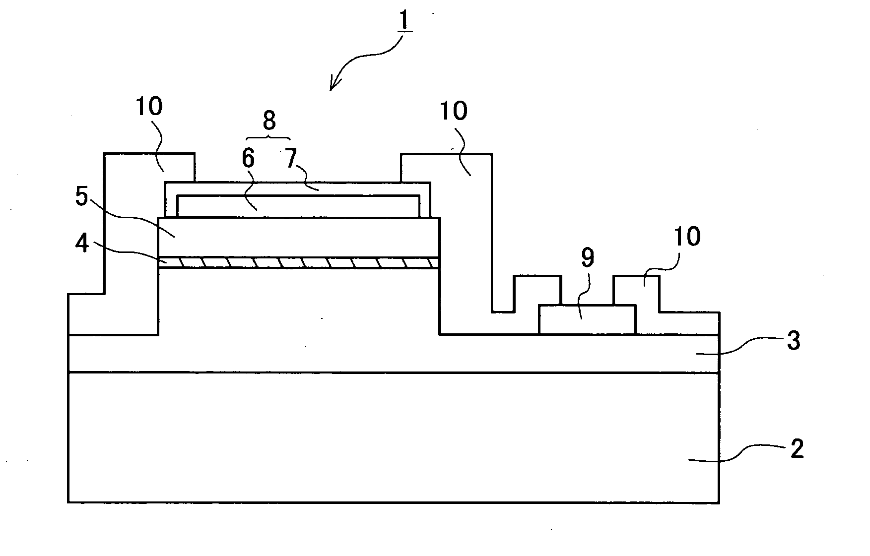
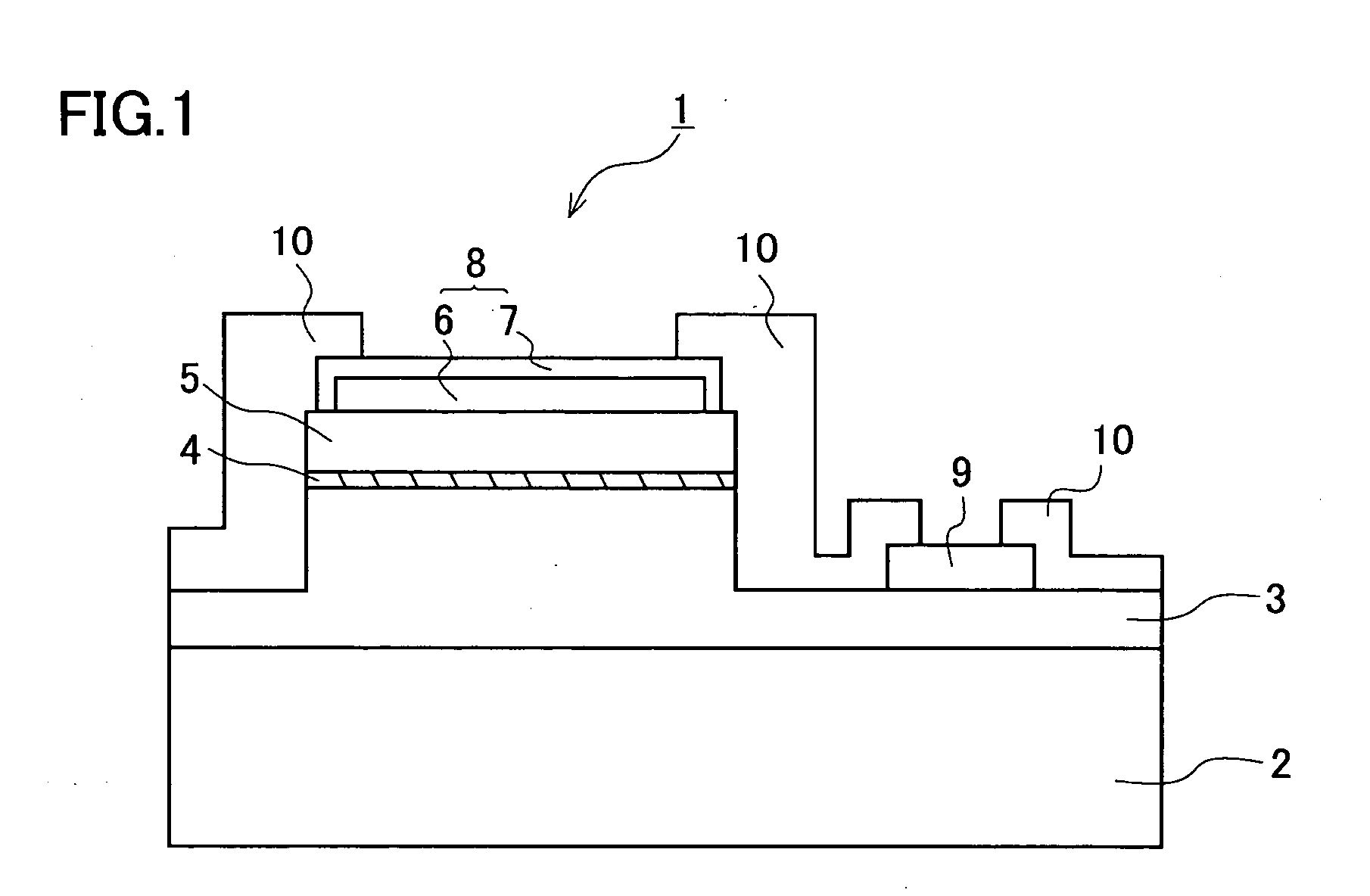
[0225]FIG. 1 illustrates the semiconductor element in this working example.

[0226] This semiconductor element 1 was configured as follows; a buffer layer (not shown) composed of Al0.1Ga0.9N and a non-doped GaN layer (not shown) were formed over a sapphire substrate 2. Over this were formed, as an n-type semiconductor layer 3 an n-type contact layer composed of silicon-doped GaN, and a super-lattice n-type clad layer produced by alternately forming a GaN layer (40 Å) and an InGaN layer (20 Å) for 10 iterations. Over this were formed a light emitting layer 4 with a multiple quantum well structure and produced by alternately forming a GaN layer (250 Å) and an InGaN layer (30 Å) for 3 to 6 iterations, and as a p-type semiconductor layer 5, a super-lattice p-type clad layer produced by alternately forming a magnesium-doped Al0.1Ga0.9N layer (40 Å) and a magnesium-doped InGaN layer (20 Å) for 10 iterations, and a p-type contact layer composed of magnesium-doped GaN, layered in that order....

working example 2

[0244] The semiconductor element of this working example was constituted the same as the semiconductor element in Working Example 1, except that a multilayer film consisting of an upper layer of platinum, a middle layer of nickel, and a lower layer of silver was formed, in a thickness of 1000 Å, 1000 Å, and 1000 Å, instead of the silver electrode in Working Example 1, and the annealing temperature after the formation of the p-electrode 8 and the n-electrode 9 was raised to about 600° C.

[0245] The semiconductor element obtained as above was connected to power under the same conditions as in Working Example 1, but the ohmic properties were still good and no migration had occurred even after 10,000 hours of continuous powered operation, meaning that a semiconductor element of high quality and reliability had been obtained.

[0246] Furthermore, the silver electrode was checked before and after power was applied, and crystal grains of about 100 nm were observed in a quantity of about 50%...

working example 3

[0248] The semiconductor element of this working example was constituted the same as the semiconductor element in Working Example 1, except that SiON was used instead of the SiN used in Working Example 2.

[0249] The performance of the semiconductor element thus obtained varied with the operating environment, but when the humidity was relatively low, for instance, the ohmic properties were just as good as in Working Example 2 in every case, and no migration occurred, meaning that a semiconductor element of high quality and reliability had been obtained.


PUM

PropertyMeasurementUnit
temperatureaaaaaaaaaa
thicknessaaaaaaaaaa
thicknessaaaaaaaaaa

Abstract

It is an object of the present invention to provide a highly reliable and high-quality semiconductor element by effectively preventing the migration of silver to a nitride semiconductor when an electrode main entirely or mostly of silver having high reflection efficiency is formed in contact with a nitride semiconductor layer. A semiconductor element comprises a nitride semiconductor layer, an electrode connected to said nitride semiconductor layer, and an insulating film covering at least part of said electrode, wherein the electrode comprises: a first metal film including silver or a silver alloy and in contact with the nitride semiconductor layer; and a second metal film completely covering the first metal film, and the insulating film comprises a nitride film.

Description

TECHNICAL FIELD [0001] The present invention relates to a semiconductor element comprised of a nitride semiconductor, and more particularly relates to an improved electrode in a semiconductor element. BACKGROUND ART [0002] In the past, the p-type electrodes in flip-chip nitride semiconductor light emitting elements have been used a structure comprised of silver or a silver alloy. Because silver very efficiently reflects the light produced by the light emitting layer of a light emitting element, such an element is able to emit light of high brightness. [0003] When silver is used for the electrode material on the p side, however, part of the silver electrode surface has to be exposed for the purpose of connection with external components and so forth, and this causes and promotes the migration of silver ions, which changes the silver at the interface with the nitride semiconductor layer, and can lead to problems such as decreased light emission intensity due to the light produced by t...

Claims


Application Information

Patent Timeline
Patent Type & Authority Applications(United States)
IPC IPC(8): H01L33/00H01L33/08H01L33/38H01L33/44
CPCH01L25/0753H01L2224/73265H01L33/20H01L33/38H01L33/40H01L33/44H01L33/08H01L2924/01322H01L2224/48465H01L2224/48247H01L2224/48091H01L2924/00H01L2924/00014H01L2924/12032
Inventor SONOBE, SHINYATOMONARI, MASAKATSUINOUE, YOSHIKI
Owner NICHIA CORP
Why Eureka
Try Eureka