Disk array device, parity data generating circuit for RAID and Galois field multiplying circuit

a parity data and array device technology, applied in the direction of digital signal error detection/correction, instruments, recording signal processing, etc., can solve the problems of data changing state, logic failure, and hardware failure, and achieve high speed

Active Publication Date: 2008-10-14
NEC CORP
View PDF6 Cites 16 Cited by
  • Summary
  • Abstract
  • Description
  • Claims
  • Application Information

AI Technical Summary

Benefits of technology

[0016]It is a first object of the present invention to provide a disk array device of RAID6 of high reliability capable of reliably guaranteeing data by parity with respect to the data, a check code of ECC even in the Galois field multiplying circuit.
[0017]It is a second object of the present invention to provide a parity data generating circuit for RAID for realizing the disk array device of RAID6 and reliably preventing the data change including a failure and checking the justifying property of the data.

Problems solved by technology

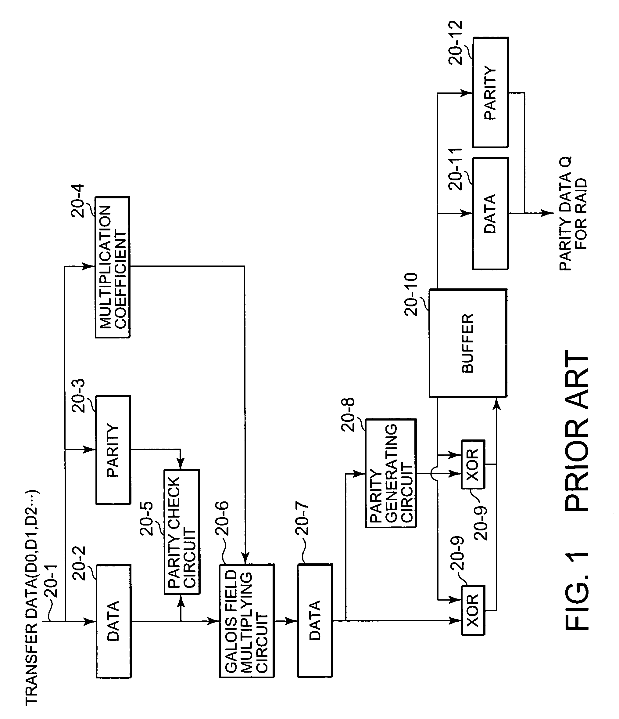
In a data guaranteeing circuit in the conventional method as shown in FIG. 1, there is an effect in a logic failure or the like.
However, no failure of hardware can be found when a breaking point is narrowed down to a certain one point as in deterioration due to a change with the passage of time within LSI (Large Scaled Integration) and a short circuit.
The parity data Q for RAID finally generated cause a data changing state, which becomes a fatal wound as a disk array system.
However, when an error signal itself showing the comparing result is broken by a short circuit, no effect can be shown at all.

Method used


Image

  • Disk array device, parity data generating circuit for RAID and Galois field multiplying circuit
  • Disk array device, parity data generating circuit for RAID and Galois field multiplying circuit
  • Disk array device, parity data generating circuit for RAID and Galois field multiplying circuit

Examples


embodiment 1

[0159]Referring to FIG. 3, a main portion of a disk array system according to an embodiment 1 of the present invention comprises a host 1, a system memory 2, a host side system bus 3 connected to the host 1 and the system memory 2, a host side IO control circuit 4 connected to the host side system bus 3, and a disk array device 5 connected to the host side IO control circuit 4.

[0160]The disk array device 5 comprises a RAID controller 6 connected to the host side IO control circuit 4, a cache memory 7 for RAID connected to the RAID controller 6, an array side system bus 8 connected to the RAID controller 6, n (n is plural) IO control circuits 9 such as SCSI (Small Computer System Interface) connected to the array side system bus 8, and n hard disk devices 10 respectively connected to each IO control circuit 9.

[0161]The RAID controller 6 includes a command processing circuit 11 connected to the host side IO control circuit 4, a data transfer control circuit 12 connected to the command...

embodiment 2

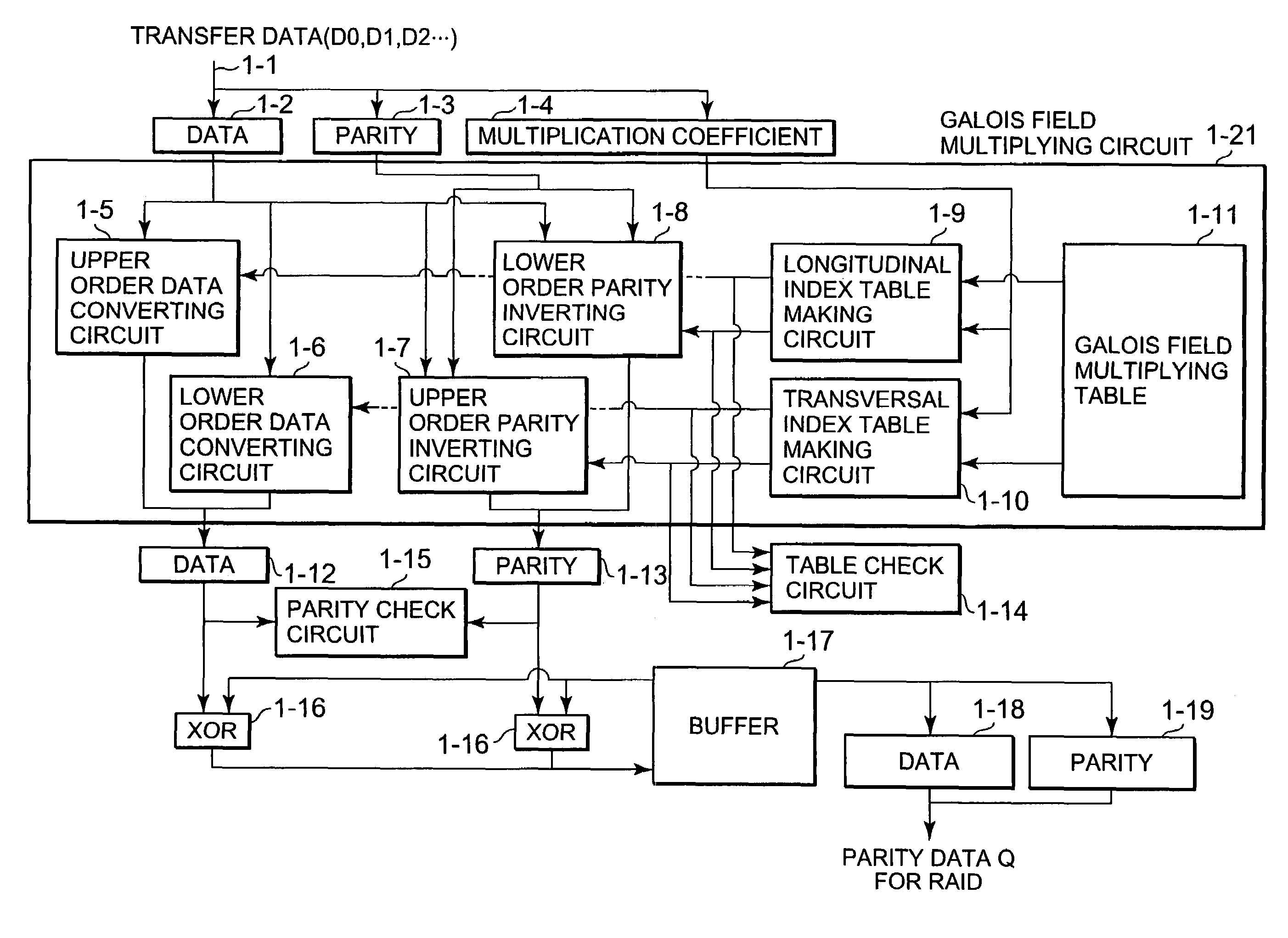
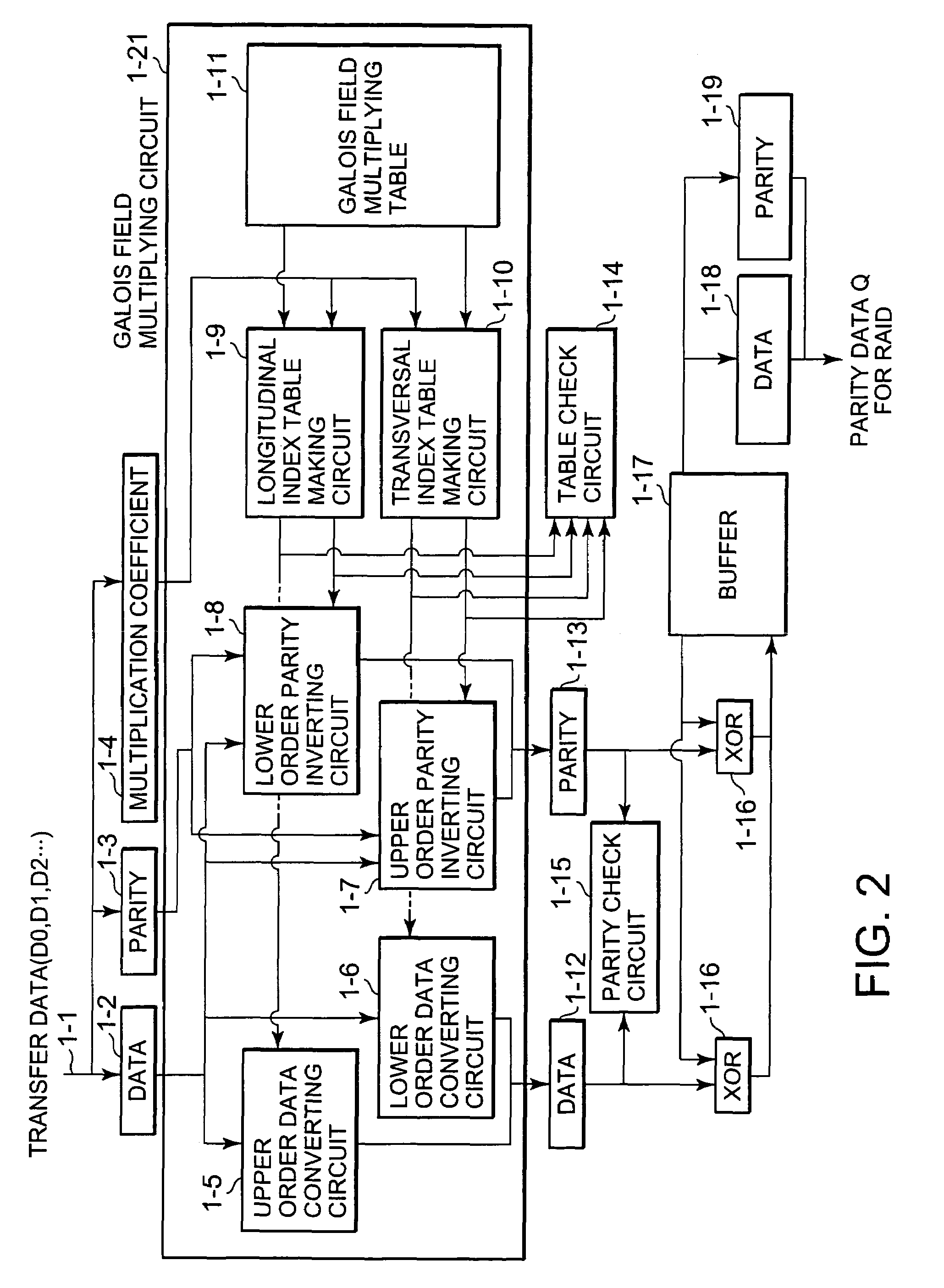
[0243]FIG. 9 is a block diagram showing the construction of a parity data generating circuit 13 for RAID in accordance with an embodiment 2 of the present invention. The basic construction of the parity data generating circuit 13 for RAID in accordance with the embodiment 2 is similar to that of the parity data generating circuit 13 for RAID in accordance with the embodiment 1 shown in FIG. 2. However, a Galois field multiplying circuit 8-21 in FIG. 9 shows a structure in which a data converting circuit portion and a parity inverting circuit portion are not divided into an upper order data portion / a lower order data portion of the data 1-2, but are divided into an odd data position / an even data position.

[0244]More specifically, the Galois field multiplying circuit 8-21 comprises a Galois field multiplying table 1-11, a longitudinal index table making circuit 1-9, a transversal index table making circuit 1-10, an even data converting circuit 8-7, an odd data converting circuit 8-8, a...

embodiment 3

[0253]FIG. 12 is a block diagram showing the construction of a parity data generating circuit 13 for RAID in accordance with an embodiment 3 of the present invention. The basic construction of the parity data generating circuit 13 for RAID in accordance with the embodiment 3 is similar to that of the parity data generating circuit 13 for RAID in accordance with the embodiment 1 shown in FIG. 2. However, the parity data generating circuit 13 for RAID in FIG. 12 is constructed when a check code is set to ECC 11-3 instead of parity. More particularly, the parity data generating circuit 13 for RAID comprises a Galois field multiplying circuit 11-21, a table check circuit 11-14, an ECC check circuit 11-15, two XOR circuits 1-16 and a buffer 1-17. The Galois field multiplying circuit 11-21 makes a Galois field multiplying calculation by inputting the data 1-2, the ECC 11-3 and the multiplication coefficient 1-4. The table check circuit 11-14 checks whether index table information generate...


PUM

PropertyMeasurementUnit
breakingaaaaaaaaaa
speedaaaaaaaaaa
poweraaaaaaaaaa

Abstract

In this parity data generating circuit, a Galois field multiplying calculation is realized by performing data conversion by index table information generated from a Galois field multiplying table so that data for RAID6 are generated. A table check circuit inspects nonconformity of the index table information in advance by using results in which the Galois field multiplying table is indexed from different directions constructed by the longitudinal direction and the transversal direction. Data and parity for making the multiplying calculation are decomposed into plural data and parities by using this table check circuit, and index table information different from each other are allocated to these data and parities. Thus, a longitudinal index table making circuit and a transversal index table making circuit themselves are checked.

Description

[0001]This application claims priority to prior application JP 2003-386997, the disclosure of which is incorporated herein by reference.BACKGROUND OF THE INVENTION[0002]1. Field of the Invention[0003]The present invention relates to a disk array device, a parity data generating circuit for RAID (Redundant Array of Independent Disks) and a Galois field multiplying circuit, and particularly, relates to a disk array device of RAID6, a parity data generating circuit for RAID and a Galois field multiplying circuit requiring high reliability and high performance.[0004]2. Description of the Related Art[0005]In the disk array device for storing important data, reliability is Increased by a RAID technique or the like conventionally known, and plural RAID systems of RAID0 to RAID5 have been defined. However, in recent years, a system of RAID6 improving these plural RAID systems has appeared and a further improvement of reliability is required.[0006]The reliability of hardware of the disk arra...

Claims


Application Information

Patent Timeline
Patent Type & Authority Patents(United States)
IPC IPC(8): G06F11/00G06F11/10G06F3/06G11B20/18G11C29/00H03M13/01H03M13/09
CPCG06F11/1076G11B20/1833G06F2211/1054G06F2211/1057
Inventor KOBAYASHI, EIJI
Owner NEC CORP
Why Eureka
Try Eureka