
FPGA having AC coupling on I/O pins with an effective bypass of the AC coupling

Active Publication Date: 2008-10-21
XILINX INC
View PDF6 Cites 5 Cited by
  • Summary
  • Abstract
  • Description
  • Claims
  • Application Information

AI Technical Summary

Benefits of technology

[0010]In accordance with embodiments of the present invention, an effective bypass of AC coupled I / O pins in an IC is used to provide good DC balance, even with an unbalanced or unknown input data signal.

Problems solved by technology

If the signal is not DC balanced, AC coupling is typically undesirable.
A new problem has therefore been created when devices with integrated AC coupling capacitors on I / O pins are targeted for applications that do not meet DC balance / run length criteria, or for input signals with unknown characteristics.
AC coupling is, thus, undesirable for such input data streams.
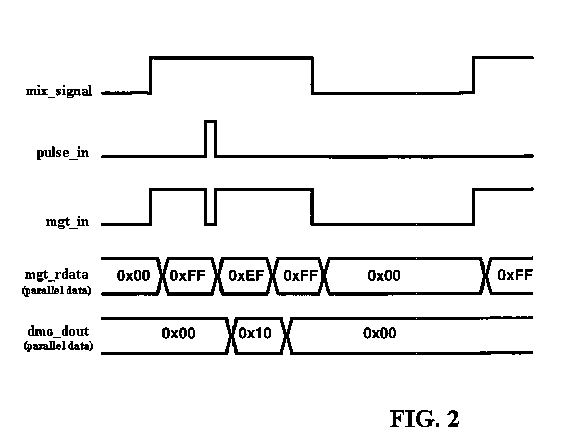
When an input data signal transitions at or near the same time as the carrier signal transition, an error can occur.

Method used


Image

  • FPGA having AC coupling on I/O pins with an effective bypass of the AC coupling
  • FPGA having AC coupling on I/O pins with an effective bypass of the AC coupling
  • FPGA having AC coupling on I/O pins with an effective bypass of the AC coupling

Examples


Embodiment Construction

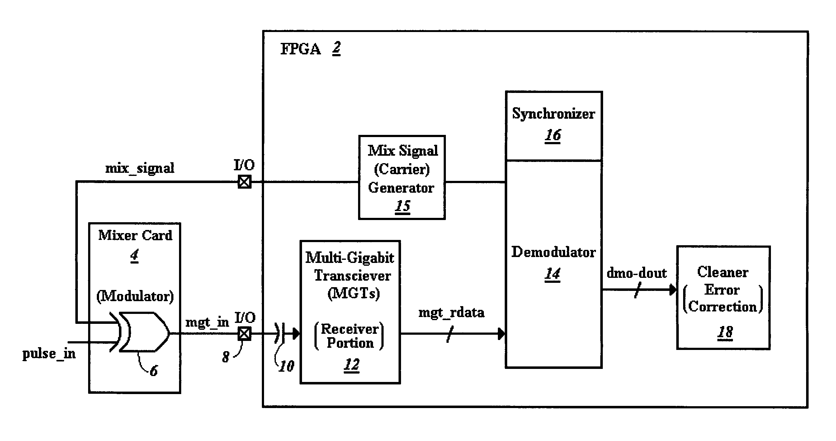
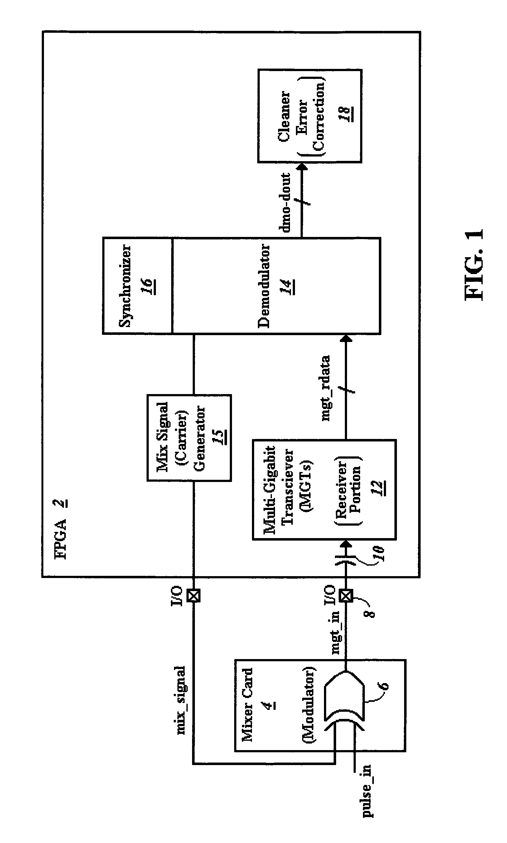
[0021]FIG. 1 illustrates a system for providing an effective bypass of AC coupling on I / O pins of an integrated circuit (IC) according to embodiments of the present invention. The IC used in the system of FIG. 1 is illustrated as a FPGA 2, although other IC types can be used. The FPGA 2 or other components containing programmable logic, such as a complex programmable logic device (CPLD), offer the advantage of logic that is programmable to form the circuitry shown in the FPGA 2 of FIG. 1. As an alternative to an IC with programmable logic, the IC can be an application specific integrated circuit (ASIC) having fixed components as shown in the FPGA 2 of FIG. 1.

[0022]In addition to the FPGA 2, the system of FIG. 1 includes a mixer card 4 with an exclusive OR (XOR) gate 6 providing a modulator for one I / O port 8 of the FPGA 2. Although not shown, the mixer card 4 can include an XOR gate for each I / O port with AC coupling where an effective bypass of the AC coupling is desired. Although ...


PUM


Abstract

DC balance is obtained in an integrated circuit (IC) having I / O pins with AC coupling by effectively bypassing the AC coupling. The DC balance is accomplished by mixing in a known, low frequency mix signal or carrier in a circuit external to the IC and then digitally canceling out that mix signal inside the IC fabric. The mixer or modulating circuitry external to the IC can be a simple XOR gate. With the IC being an FPGA, the logic internal to the FPGA can be programmed to form the demultiplexing circuitry to digitally cancel out the mix signal, as well as to provide a carrier signal to the external mixer. To minimize errors due to data signal transitions near the edge of the carrier signal, a cleaner circuit is used to eliminate transitioning bits on either side of a carrier signal edge. With modulation used, synchronization circuitry is likewise included to provide synchronization during startup as well as after long dead times in the data signal.

Description

BACKGROUND[0001]1. Technical Field[0002]The present invention relates to integrated circuits (ICs) with AC coupling on the I / O pins, where DC balance is desired for at least some data signals provided to the I / O pins. More particularly, the present invention relates to providing a bypass to the AC coupling to enable DC balance of an input data signal.[0003]2. Related Art[0004]AC-coupling is desirable for a number of reasons—(1) To change the DC bias level when interconnecting logic families with different switching thresholds; (2) To provide a removable interface that may be shorted to ground without damaging the output drivers; or (3) When combined with differential signaling and transformer coupling, to connect boxes without requiring any DC connection between the two product chassis.[0005]AC coupling is typically accomplished using a high-pass filter placed in series with a transmission line. A series-connected DC-blocking capacitor is a good example of a commonly used high-pass ...

Claims


Application Information

Patent Timeline
IPC IPC(8): H04L5/16
CPCH04L25/0268H04L25/0292
Inventor HAGEN, TIMOTHY P.
Owner XILINX INC
Learn More