Wavelength selective photonics device

a selective photonics and wavelength technology, applied in the direction of superconductor devices, radiation controlled devices, semiconductor lasers, etc., can solve the problems of increasing the number of wavelengths, unable to guarantee the desirable filtering of all carriers in all, and becoming impractical

Inactive Publication Date: 2008-10-28
QUANTUM SEMICON
View PDF6 Cites 11 Cited by
  • Summary
  • Abstract
  • Description
  • Claims
  • Application Information

AI Technical Summary

Problems solved by technology

However, this solution becomes impractical as the number of wavelengths increases.
Unfortunately, the solution suggested in that patent application does not guarantee the desirable filtering for all carriers in all circumstances.

Method used


Image

  • Wavelength selective photonics device
  • Wavelength selective photonics device
  • Wavelength selective photonics device

Examples


Embodiment Construction

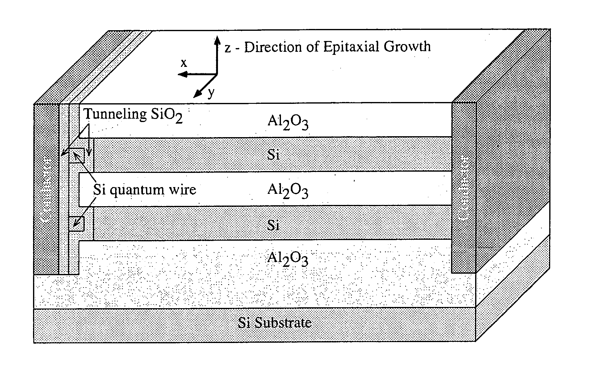
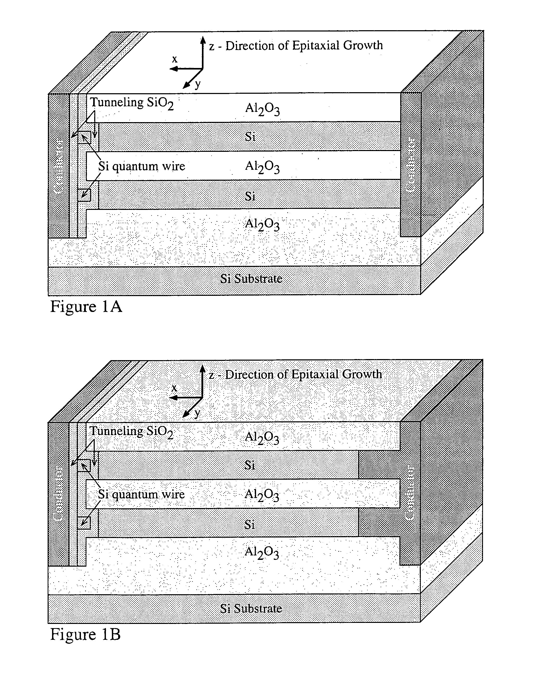
[0047]FIG. 1A and FIG. 1B, show two exemplary implementations of the lateral contacts for light emission for interband or intersubband transitions. The implementations include on the left hand side of the stack a novel Quantum Wire Injector (QWI) architecture that is especially useful for light emission through intersubband transitions, both n-type and p-type. The two implementations differ only in the geometry of the “Extractor” contact located on the right hand side of the stack. The geometry of the Extractor contact does not alter the physics or the operation of the device. In these two figures, the conductors used for the QWI and for the extractor are not defined. These conductors can be metals, highly doped semiconductors, or conductive metal-oxides, for example. Band diagrams will illustrate the impact of choosing different conductors.

[0048]The QWI as shown in FIG. 1A and FIG. 1B on the left hand side of the structures, is composed of a Si quantum wire encapsulated in an insul...


PUM


Abstract

A device comprising a number of different wavelength-selective active-layers arranged in a vertical stack, having band-alignment and work-function engineered lateral contacts to said active-layers, consisting of a contact-insulator and a conductor-insulator. Photons of different energies are selectively absorbed in or emitted by the active-layers. Contact means are arranged separately on the lateral sides of the vertical stack for injecting charge carriers into the photon-emitting layers and extracting charge carriers generated in the photon-absorbing layers. The device can be used for various applications for light emission or light absorption. The stack of active layers may also include top and bottom electrodes whereby the device can also be operated as a FET device.

Description

[0001]This application is a continuation-in-part of U.S. patent application Ser. No. 10 / 023,430 filed on Dec. 14, 2001, which is a continuation-in-part of PCT / EP00 / 05590 filed Jun. 13, 2000, which claims the benefit of U.S. provisional patent application 60 / 140,671 filed Jun. 14, 1999.BACKGROUND OF THE INVENTION[0002]The present invention relates to the field of opto-electronic or photonic devices, including photon-absorption and photon-emission processes. U.S. patent application Ser. No. 10 / 023,430 discloses an opto-electronic device architecture that can be implemented in different materials systems, including silicon and germanium. The essential features of that device architecture are the fabrication of an epitaxial film stack composed of alternating layers of a semiconductor (e.g. Si or Ge) and materials with wide band-gaps that can be made pseudomorphic with respect to the lattice parameter of the semiconductor (Si or Ge). Stacked Quantum Wells (QWs) and short-period SuperLatt...

Claims


Application Information

Patent Timeline
Patent Type & Authority Patents(United States)
IPC IPC(8): H01L33/00H01L27/14H01L27/146H01L31/02H01L31/0216H01L31/028H01L31/0328H01L31/0352H01L33/06H01L33/08H01S5/00
CPCB82Y20/00H01L31/035236H01L27/14601H01L27/1462H01L27/14625H01L31/02162H01L31/028H01L33/06H01L33/08
Inventor AUGUSTO, CARLOS J. R. P.
Owner QUANTUM SEMICON
Why Eureka
Try Eureka