Boost DC-DC converter and semiconductor device having boost DC-DC converter

a technology of dc-dc converter and converter, which is applied in the direction of dc-dc conversion, power conversion system, instruments, etc., can solve the problem that the conventional boost dc—dc converter cannot be actuated

Active Publication Date: 2008-10-28
ABLIC INC
View PDF9 Cites 116 Cited by
  • Summary
  • Abstract
  • Description
  • Claims
  • Application Information

AI Technical Summary

Benefits of technology

[0011]With the above-described structure, it is possible to attain a boost DC—DC converter which is actuated at power supply voltage lower than that necessary for actuating the above-described conventional boost DC—DC converter.
[0013]Similarly to the first aspect of the present invention, with the above-described structure, it is possible to attain a boost DC—DC converter which is actuated at power supply voltage lower than that necessary for actuating the above-described conventional boost DC—DC converter.

Problems solved by technology

As described above, in starting a conventional boost DC—DC converter, there is a problem in that the conventional boost DC—DC converter cannot be actuated unless the input voltage of power supply that is higher than the lowest voltage at which the internal booster circuit can be actuated by Vf of the Schottky diode is inputted.

Method used


Image

  • Boost DC-DC converter and semiconductor device having boost DC-DC converter
  • Boost DC-DC converter and semiconductor device having boost DC-DC converter
  • Boost DC-DC converter and semiconductor device having boost DC-DC converter

Examples


embodiment 1

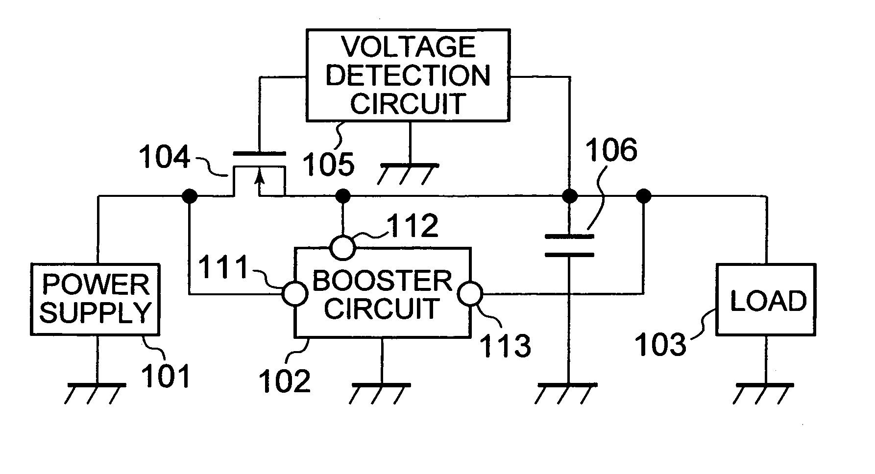
[0023]FIG. 1 illustrates a semiconductor device having a boost DC—DC converter according to a first embodiment of the present invention.

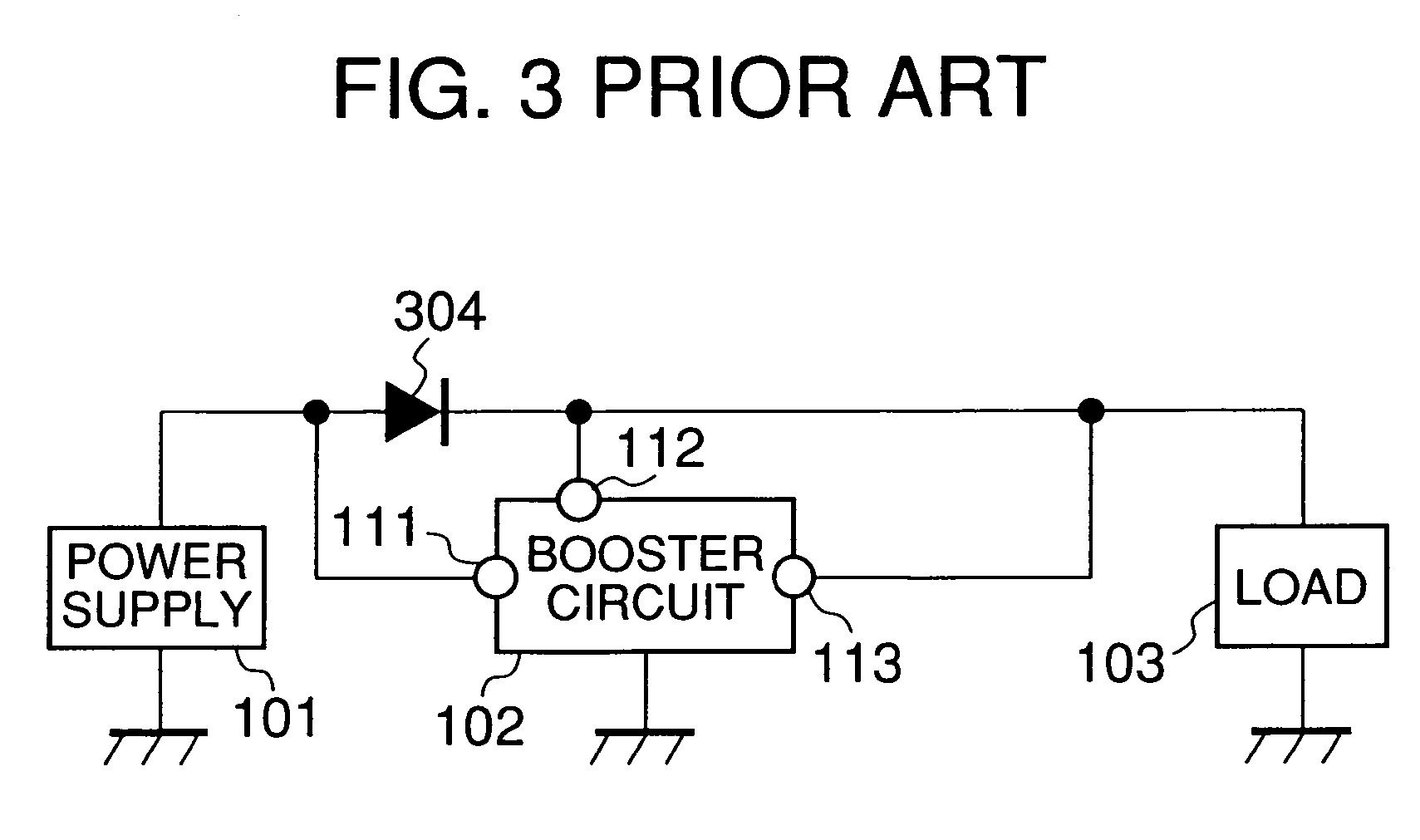
[0024]As illustrated in FIG. 1, instead of the Schottky diode used in the conventional structure of a boost DC—DC converter, a p-channel MOS transistor (hereinafter briefly referred to as PMOS) 104 as a switching device is provided. Further, additionally provided to the conventional structure of a boost DC—DC converter are a voltage detection circuit 105 for detecting voltage at a power supply terminal 112 of a booster circuit 102 to control on / off of the PMOS 104 according to a result of the detection and a storage capacitor 106 for storing electric power such that the stored electric power can operate the booster circuit 102 for a predetermined length of time even when electric power is stopped being supplied to the power supply terminal 112 of the booster circuit 102. The PMOS 104 is connected in series between an input terminal 111 of the booste...

embodiment 2

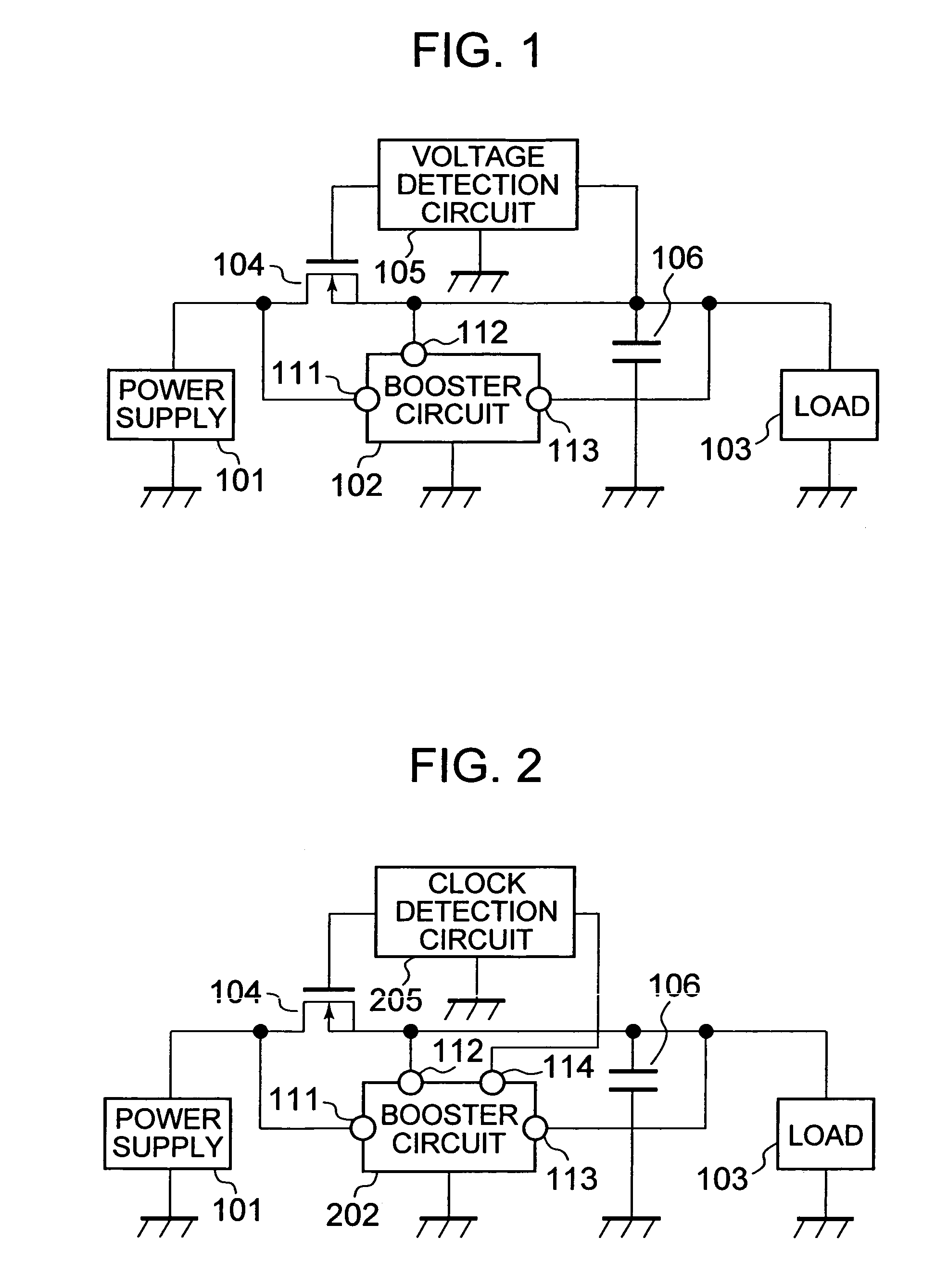
[0030]FIG. 2 illustrates a semiconductor device having a boost DC—DC converter according to a second embodiment of the present invention.

[0031]As illustrated in FIG. 2, instead of the booster circuit 102 of the boost DC—DC converter and the voltage detection circuit 105 of the first embodiment illustrated in FIG. 1, a booster circuit 202 which is the booster circuit 102 having a clock output terminal 114 attached thereto for outputting a clock signal of an internal oscillation circuit of the booster circuit 102, and a clock detection circuit 205 for turning off the PMOS 104 when the frequency of a clock signal outputted from the clock output terminal 114 of the booster circuit 202 is equal to or higher than a first frequency that is slightly higher than the lowest frequency at which the booster circuit 202 can generate the boosted electric power and turning on the PMOS 104 when the frequency of the clock signal is lower than the lowest frequency at which the booster circuit 202 can ...


PUM


Abstract

Provided is a boost DC-DC converter where electric power to be supplied to a booster circuit is supplied from a power supply and from boosted electric power of the booster circuit which can be actuated at a low voltage. The boost DC-DC converter has a structure in which: a switching device is provided between the power supply and a boosted output of the booster circuit; a storage capacitor for storing electric power to be inputted to the booster circuit and for operating the booster circuit for a predetermined length of time using the stored electric power is additionally provided; and in a case where the booster circuit can generate boosted electric power even when the switching device is turned off, the switching device is turned off.

Description

[0001]This application claims priority under 35 U.S.C. § 119 to Japanese Patent Application No 2005-132521 filed Apr. 28, 2005, the entire content of which is hereby incorporated by reference.BACKGROUND OF THE INVENTION[0002]1. Field of the Invention[0003]The present invention relates to a semiconductor device having a boost DC—DC converter for converting input electric power to output electric power having a voltage higher than that of the input electric power. In particular, the present invention relates to a semiconductor device having a boost DC—DC converter that operates at the output voltage when actuated.[0004]2. Description of the Related Art[0005]FIG. 3 illustrates a semiconductor device having a conventional boost DC—DC converter.[0006]As illustrated in FIG. 3, the semiconductor device includes: a power supply 101; a booster circuit 102 for converting electric power supplied by the power supply 101 to electric power having higher voltage; a Schottky diode 304; and a load 1...

Claims


Application Information

Patent Timeline
Patent Type & Authority Patents(United States)
IPC IPC(8): G05F1/00
CPCH02M3/156H02M3/07H02M3/155
Inventor UTSUNOMIYA, FUMIYASU
Owner ABLIC INC
Why Eureka
Try Eureka