

Surface plasmon resonance sensor
a surface plasmon and sensor technology, applied in the field of surface plasmon resonance (spr) sensors, can solve the problems of reducing the possibility of contamination of fluids pumped through the flow cell, and reducing the cost of production
- Summary
- Abstract
- Description
- Claims
- Application Information
AI Technical Summary
Benefits of technology
Problems solved by technology
Method used
Image

Examples
Embodiment Construction
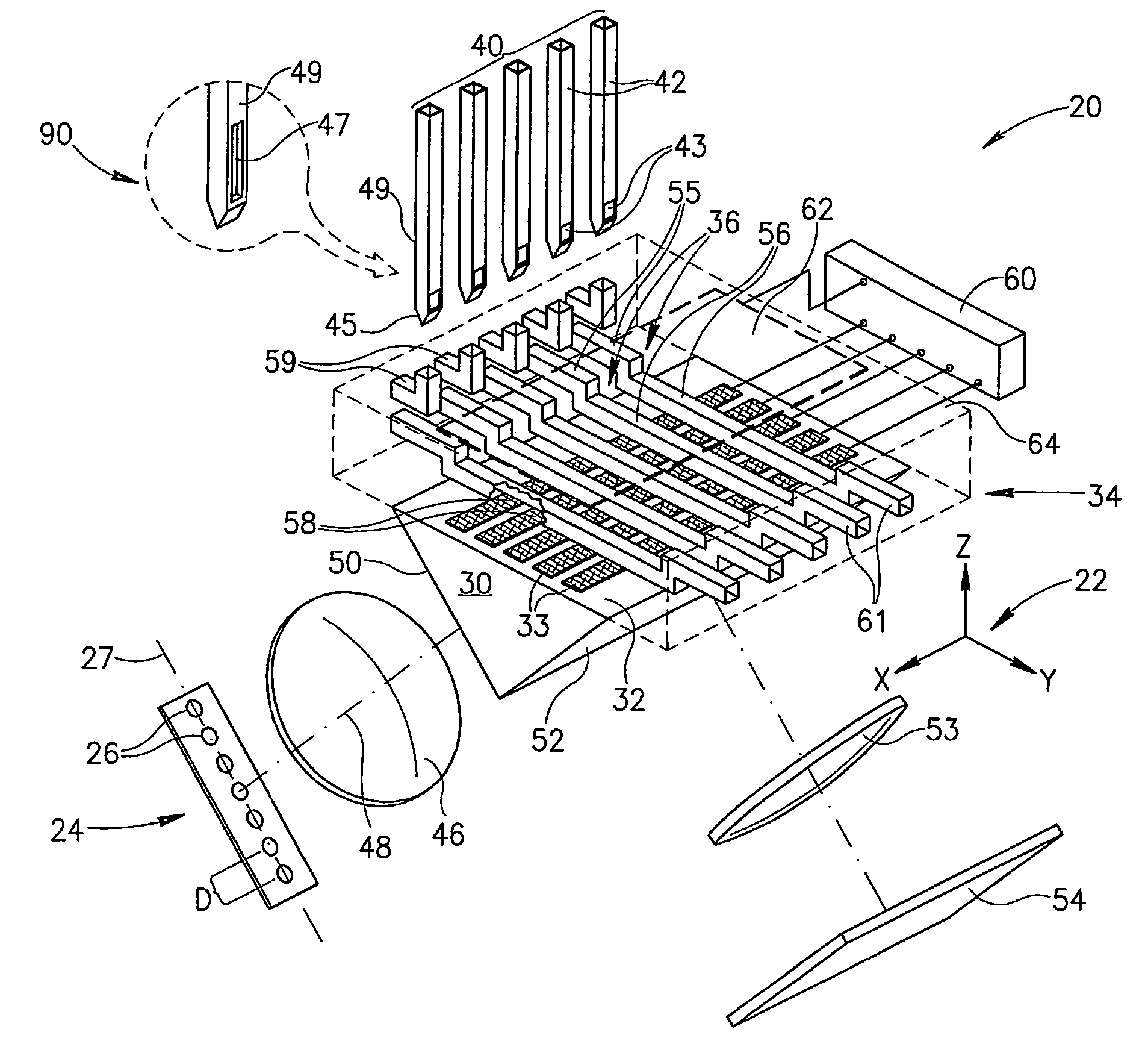
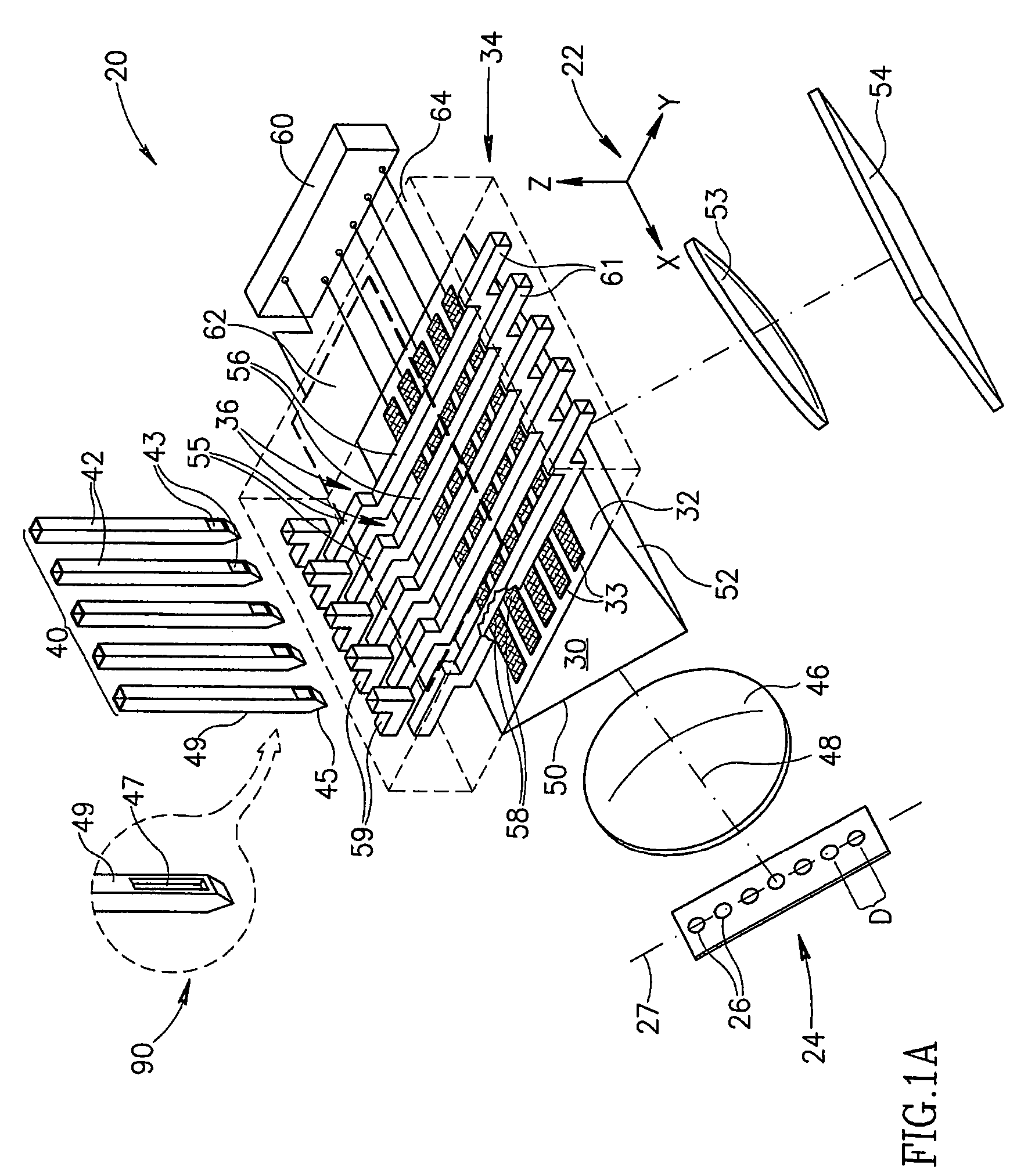
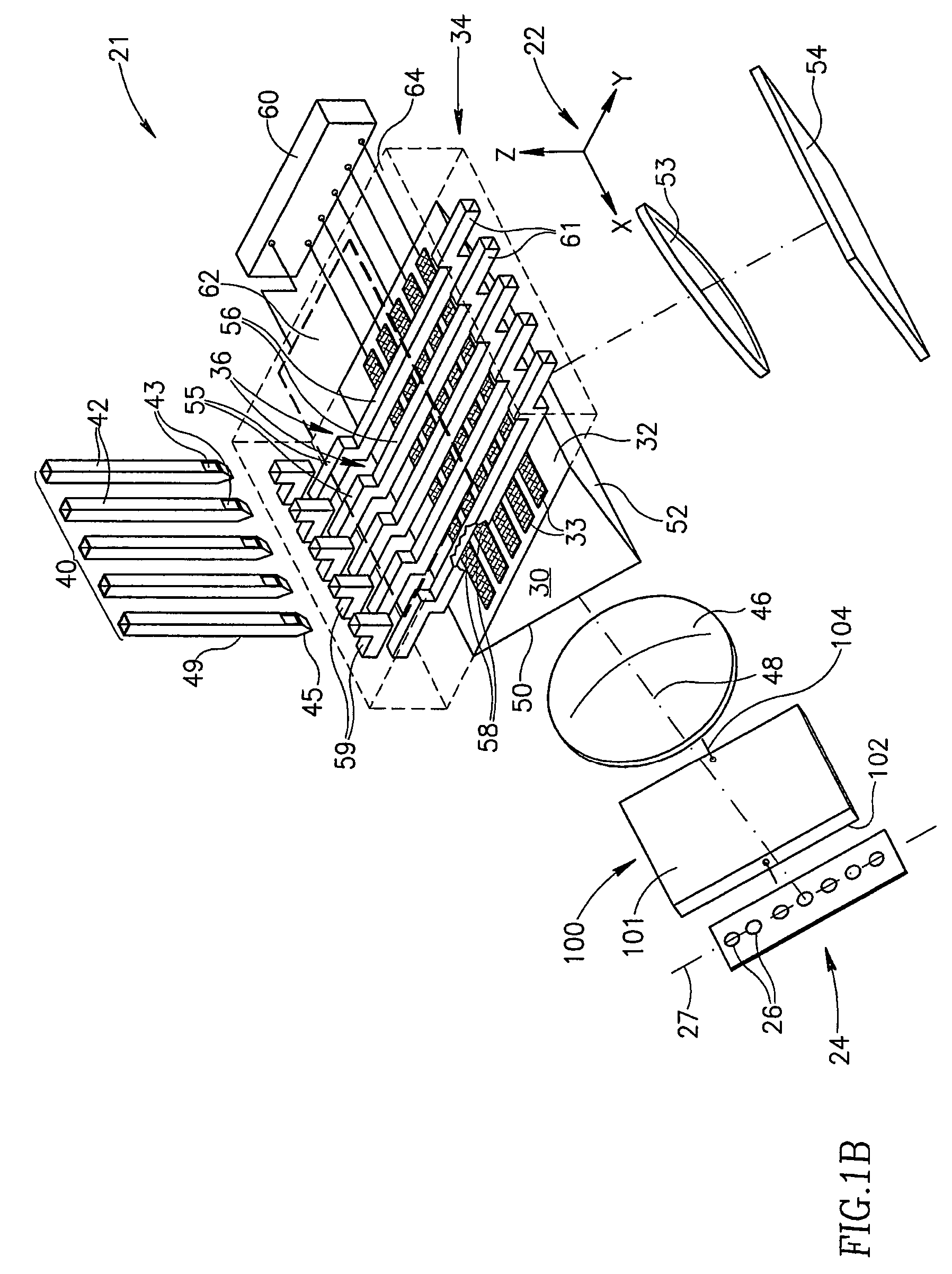
[0074]FIG. 1A schematically shows an SPR sensor 20 in accordance with an embodiment of the present invention. For convenience of discussion location and position of elements and features of SPR sensor 20 are referred to a coordinate system 22.
[0075]SPR sensor 20 comprises an optionally linear array 24 of light sources 26 having an array axis 27 and a prism 30 having a sensor surface 32. A flow cell 34 comprises microchannels 36 for flowing liquid across and in contact with sensor surface 32 and a probe layer (not shown) of desired ligands generated on a suitable SPR conductor formed on the sensor surface. In SPR sensor 20 the probe layer is generated on an SPR conductor optionally comprising a plurality of strip electrodes 33.
[0076]An array 40 of flow needles 42 coupled to suitable pumping apparatus (not shown) is optionally used to introduce liquids into microchannels 36. Operation of flow needles 42 in introducing liquid into microchannels 36 is described below. Microchannels 36 a...
PUM
| Property | Measurement | Unit |
|---|---|---|
| dimension | aaaaa | aaaaa |
| dimension | aaaaa | aaaaa |
| dimension | aaaaa | aaaaa |
Abstract
Description
Claims
Application Information