Conversion device for performing a raster scan conversion between a JPEG decoder and an image memory

a conversion device and raster scan technology, applied in the field of image processing, can solve the problems of time-consuming, central processing unit real-time problems, and the inability to use macroblocks directly by the display functionality, so as to speed up the raster scan conversion and increase the memory access efficiency. , the effect of saving cpu tim

Inactive Publication Date: 2008-12-02
STMICROELECTRONICS PVT LTD +1
View PDF6 Cites 2 Cited by
  • Summary
  • Abstract
  • Description
  • Claims
  • Application Information

AI Technical Summary

Benefits of technology

[0005]Objects of the invention include: addressing the above described problem; saving the CPU time and speeding up the raster scan conversion; and increasing the memory access efficiency and reaching the maximum theoretical data bandwidth of a memory whatever the data bus size.
[0009]Thus, the approach of the invention is fully hardwired and no software is required. Consequently, the CPU time is saved and the raster scan conversion is sped up due to hardware acceleration. Further, memory access efficiency is increased as, according to the invention, the whole memory data bus is used. In other words, whatever the data bus size, the maximum theoretical data bandwidth is reached.

Problems solved by technology

Unfortunately, these macroblocks cannot be used directly by the display functionality.
However, such an approach is time consuming and can generate real time issues for the central processing unit.

Method used


Image

  • Conversion device for performing a raster scan conversion between a JPEG decoder and an image memory
  • Conversion device for performing a raster scan conversion between a JPEG decoder and an image memory
  • Conversion device for performing a raster scan conversion between a JPEG decoder and an image memory

Examples


Embodiment Construction

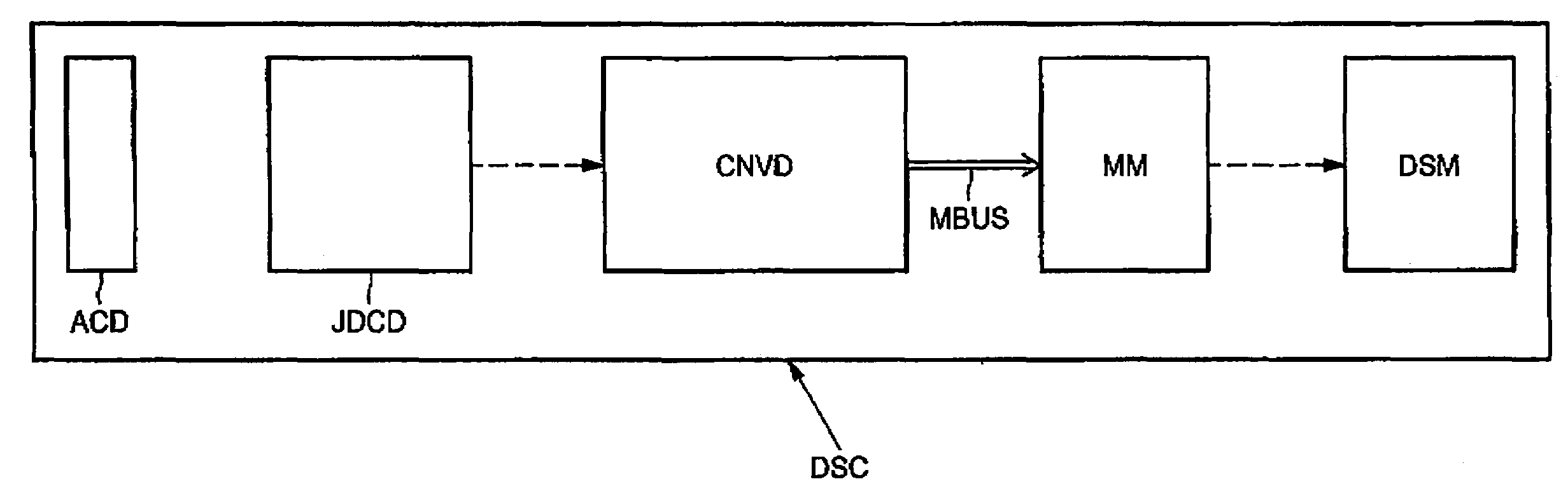
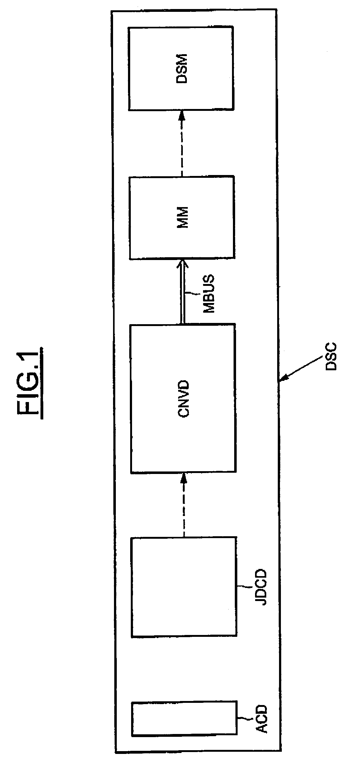
[0027]In FIG. 1, DSC designates a Digital Still Camera including an optical acquisition device ACD. A conventional JPEG decoder JDCD is responsible for reading encoded data in a memory (not represented in this figure) and converting the data into interleaved 8×8 macroblocks of the color components. A conversion device according to the invention CNVD is connected between the output of the JPEG decoder JDCD and an image memory MM and is adapted for performing a raster scan conversion between the JPEG decoder and the image memory MM which is adapted to contain the reconstructed final image to be displayed on a display module DSM.

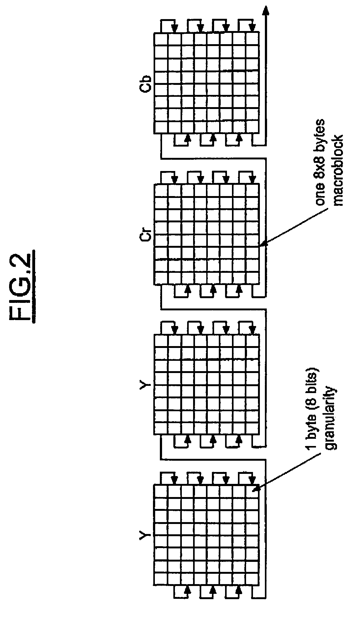
[0028]Further, the image memory MM is connected to the output of the conversion device CNVD by a memory data bus MBUS which has a size, for example 16 bits, corresponding to the bandwidth of the image memory (i.e. the number of bits which can be written simultaneously in the image memory). As illustrated in FIG. 2, the JPEG decoder first generated two macrobloc...


PUM


Abstract

The conversion device includes an input for receiving data corresponding to an image to be displayed. The received data is in a JPEG decoder output data format A processor is included for reconstructing and writing the image to be displayed into the image memory, in a display module expected input data format. The bandwidth of the image memory is greater than one byte. The processor is fully hardwired and includes a first logic stage for writing the received data byte by byte into an intermediate memory at chosen addresses such that the written data form a sequence of data in the display module expected input data format, and a second logic stage for reading the written data in the intermediate memory, forming successive packets of read data having a size corresponding to the bandwidth, and successively writing the packets into the image memory at chosen addresses such that the written packets together form all the lines of the image.

Description

FIELD OF THE INVENTION[0001]The present invention relates to image processing, especially JPEG decoding, and in particular to a raster scan conversion between a JPEG decoder and an image memory, for example, for Digital Still Cameras (DSC).BACKGROUND OF THE INVENTION[0002]A JPEG decoder is responsible for reading encoded data and converting the data into interleaved 8×8 macroblocks of the color components (i.e. luminance Y and chrominance Cr, Cb). More precisely, when an image to be displayed is decoded by the JPEG decoder, the JPEG decoder will first generate two macroblocks of luminance Y, then one macroblock of chrominance Cb and then one macroblock of chrominance Cr.[0003]Unfortunately, these macroblocks cannot be used directly by the display functionality. Indeed, the display functionality is expecting a raster scan format, i.e. Y data for first pixel followed by Cr for adjacent pixel, and then Y of second pixel followed by Cb of first and second pixels (there is only one Cb an...

Claims


Application Information

Patent Timeline
Patent Type & Authority Patents(United States)
IPC IPC(8): G06K9/36H04N7/26H04N7/30
CPCH04N19/85H04N19/60H04N2201/33378
Inventor GAUTIER, ANTOINECHANDRA, MAHESH
Owner STMICROELECTRONICS PVT LTD
Why Eureka
Try Eureka