Electro-optical display device and image projection unit

a display device and optical display technology, applied in the field of optical display devices, can solve problems such as the degradation of the contrast ratio of the lcd device, and achieve the effect of suppressing the reduction of the contrast ratio and brightness of the electro-optical display devi

Inactive Publication Date: 2008-12-23
VISTA PEAK VENTURES LLC
View PDF11 Cites 10 Cited by
  • Summary
  • Abstract
  • Description
  • Claims
  • Application Information

AI Technical Summary

Benefits of technology

[0013]It is an object of the present invention to provide an elector-optical device, such as an LCD device, capable of suppressing reduction of the contrast ratio and brightness of the electro-optical display device caused by the light refracted toward the interconnections and TFTs after passing through the opening area of the pixel, by using an technique other than the techniques proposed by the publications as described above.
[0021]In accordance with the electro-optical display device of the first aspect of the present invention, the incident light incident within the opening area of the pixel is effectively used for the pixel without being incident onto the shielded element, thereby improving the brightness of the electro-optical display device. In addition, since shielded element, such as the TFT, is not irradiated by the incident light, the shielded element does not cause any leakage current to thereby improve the contrast ratio of the electro-optical display device.
[0023]In accordance with the electro-optical display device of the second aspect of the present invention, since the refractive indexes of the each two of the insulation films in the opening area which have interfaces therebetween not parallel to the first substrate are equivalent to one another, the light incident onto the slope portion travels in the same direction as the direction of the incident light without refraction. This suppresses the incidence of the light onto the shielded element such as TFT and interconnections, thereby improving the brightness and the contrast ratio of the electro-optical display device.

Problems solved by technology

In addition, the light, if it is incident onto the channel of the TFT, generates a leakage current flowing through the TFT during the OFF state thereof, thereby degrading the contrast ratio of the LCD device.

Method used


Image

  • Electro-optical display device and image projection unit
  • Electro-optical display device and image projection unit
  • Electro-optical display device and image projection unit

Examples


first embodiment

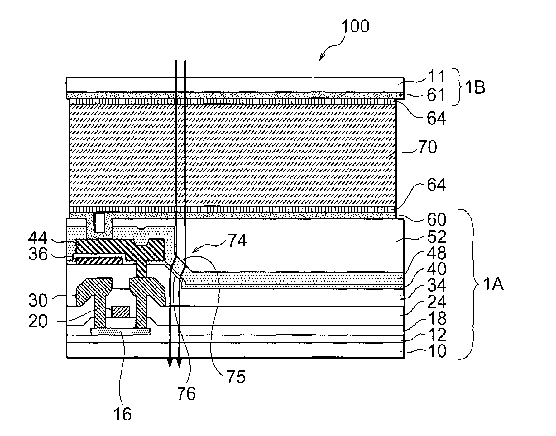
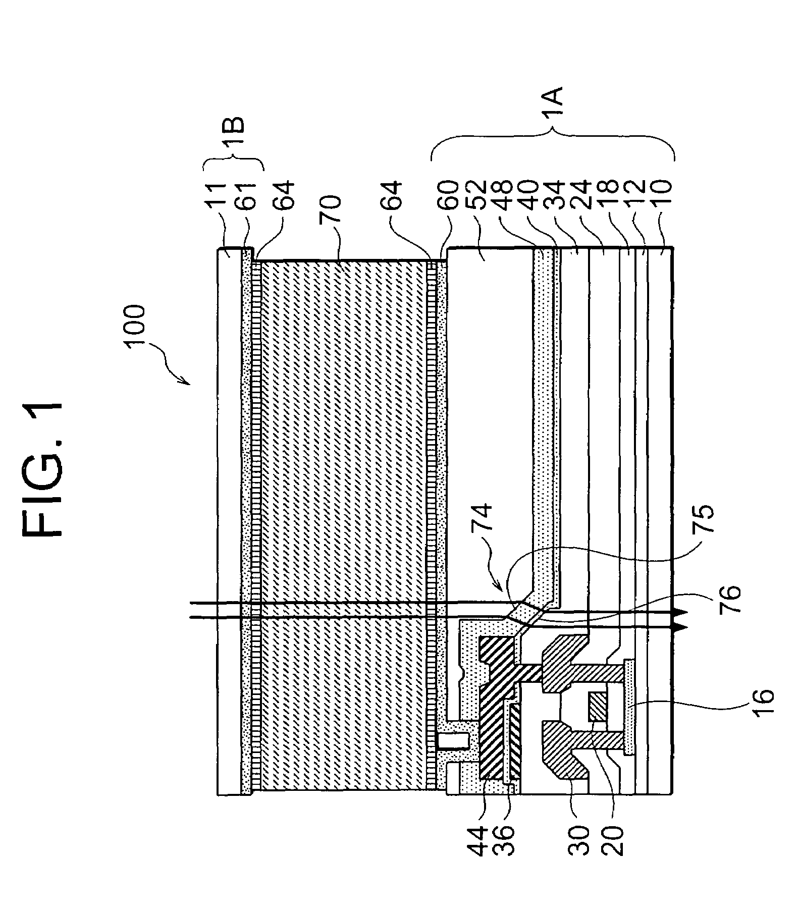
[0041]Referring to FIG. 1, a transmission LCD device, generally designated by numeral 100, according to the electro-optical display device of the present invention, includes a TFT substrate 1A and a counter substrate 1B sandwiching therebetween an LC layer 70. The TFT substrate 1A includes a glass substrate body 10, and a base layer 12 made of silicon oxide formed on the glass substrate body 10 and having a thickness of 0.06 to 0.03 μm. The base layer 12 has a function of preventing TFTs formed thereon from being stained by impurities diffused from the glass substrate body 10.

[0042]The TFTs formed on the base layer 12 each includes a polysilicon layer 16 acting as an active layer for the TFT, a gate electrode formed as a part of gate line 20, and a gate insulation film 18 formed between the polysilicon layer 16 and the gate line 20. The gate line 20 is made of WSi, Cr or Al, for example. The gate insulation film 18 is made of silicon oxide having a thickness of 0.1 μm. A portion of ...

second embodiment

[0067]Referring to FIG. 4, a transmission LCD device, generally designated by numeral 200, according to the present invention is similar to the LCD device of FIG. 1 except for the layered structure. More specifically, in the LCD device of the present embodiment, the capacitor shown in FIG. 1 is not formed, and the third interlayer dielectric film 48 is formed directly on the second interlayer dielectric film 34. A through hole is formed penetrating the organic planarization film 52, the third interlayer dielectric film 48 and the second interlayer dielectric film 34 to reach the source / drain line 30. The pixel electrode 60 is formed on the organic planarization film 52 and in the through hole.

[0068]In the counter substrate 1B, a shield film pattern 44 is formed to shield the TFT area in the TFT substrate 1A, replacing a portion of the orientation film 64. Other configurations of the LCD device 200 are similar to those of the LCD device 100 of FIG. 1.

[0069]FIGS. 5J to 5M show fabrica...

third embodiment

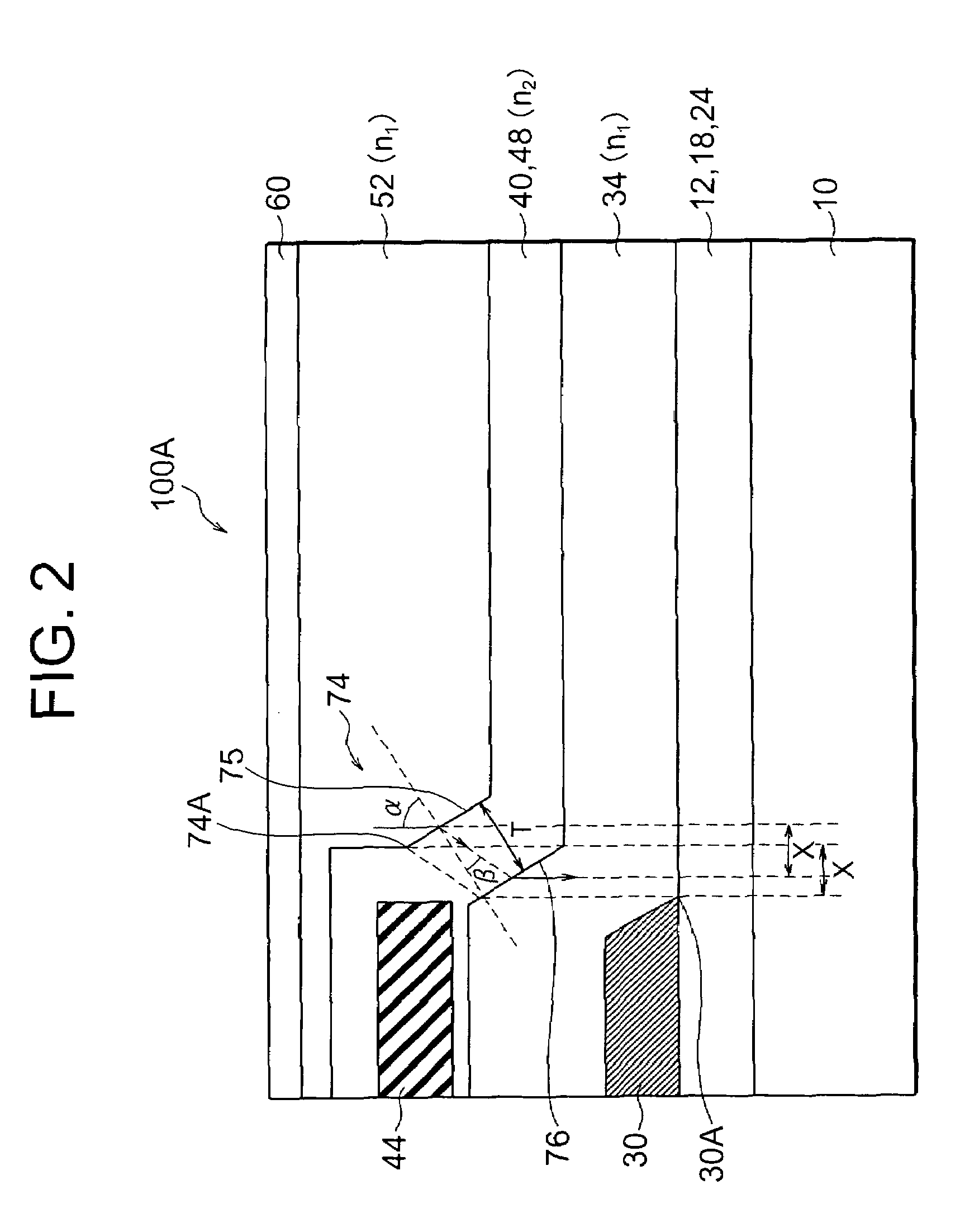
[0073]Referring to FIG. 6, a TFT substrate 3A of a transmission LCD device according to the present invention is such that portions of the third interlayer dielectric film 48 and the capacitor insulation film 40 located within the opening area, or inner side of the slope area 74, are removed by etching. On the portion of the second interlayer dielectric film 34 exposed by the removal of the third interlayer dielectric film 48 and on the remaining portion of the third interlayer dielectric film 48, there is provided an organic planarization film 52 made of silicone resin. The organic planarization film 52 has a flat top surface parallel to the surface of the glass substrate body 10. The organic planarization film 52 has a refractive index of about 1.4 to 1.5, which is equivalent to the refractive index of the glass substrate body 10 and the silicon oxide. A through hole 56 is formed penetrating the organic planarization film 52 and the third interlayer dielectric film 48 to reach the...


PUM

PropertyMeasurementUnit
surface roughnessaaaaaaaaaa
thicknessaaaaaaaaaa
thicknessaaaaaaaaaa

Abstract

An LCD device includes a plurality of pixels each having a slope area configured by a plurality of layers. A shielded element shielded by a black matrix has an inner edge located at a distance X apart from the outer edge of the slope area, the distance X being expressed by the formula: x=(T1 / cos β)×sin(α−β), wherein α and β are incidence angle and refracted angle, respectively, of the incident light at an interface between the layers having different refractive indexes in the slope area, and T1 is a thickness of the underlying layer forming the interface.

Description

BACKGROUND OF THE INVENTION[0001](a) Field of the Invention[0002]The present invention relates to an electro-optical display device and, more particularly, to an electro-optical display device, such as a liquid crystal display (LCD device), for displaying an image by using an electro-optical effect. The present invention also relates to an image projection unit having such an electro-optical display device.[0003](b) Description of the Related Art[0004]Some electro-optical display devices such as a liquid crystal display (LCD) device are used as image display units of a direct view type in a variety of equipment, or light valves of image projection units. The electro-optical display device generally includes an electro-optical substance layer such as a liquid crystal (LC) layer and a pair of substrates sandwiching therebetween the electro-optical substance layer. One of the substrates, a TFT substrate, mounts thereon an array of pixels each including a pixel electrode and a switching...

Claims


Application Information

Patent Timeline
Patent Type & Authority Patents(United States)
IPC IPC(8): G02F1/1333G02F1/13G02F1/1362G02F1/1368G09F9/30H01L21/336H01L29/786
CPCG02F1/133345G02F1/136209G02F2201/40
Inventor SHIOTA, KUNIHIROTANABE, HIROSHI
Owner VISTA PEAK VENTURES LLC
Why Eureka
Try Eureka