Organic light emitting diode display and method for manufacturing the same

Active Publication Date: 2009-05-21
SAMSUNG DISPLAY CO LTD
View PDF10 Cites 25 Cited by
  • Summary
  • Abstract
  • Description
  • Claims
  • Application Information

AI Technical Summary

Benefits of technology

[0042]Accordingly, the driving voltage lines overlap the gate lines and the data lines such that the emission area may be increased by an amount of an area that the driving voltage lines occupy, thereby increasing the aperture ratio.
[0043]Also, the driving voltage lines are not neighboring the gate lines and the data lines, and are vertically departed therefrom via the passivation layer made of organic insulator such that mutual influences between the gate voltages, the data voltages, and the driving voltages are decreased, thereby preventing the signal delay.
[0044]In addition, the driving voltage lines do not intercept the gat

Problems solved by technology

However, because the LCD is a passive display device, an additional back-light as a light source is needed, and the LCD has various problems such as a slow response time and a narrow viewing angle.
However, the driving vol

Method used


Image

  • Organic light emitting diode display and method for manufacturing the same
  • Organic light emitting diode display and method for manufacturing the same
  • Organic light emitting diode display and method for manufacturing the same

Examples


exemplary embodiment 1

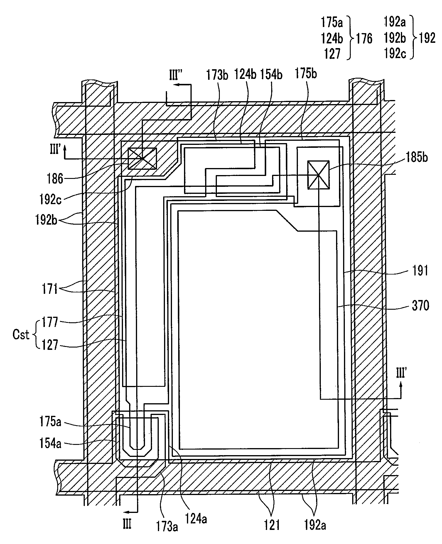
[0058]Now, an OLED display according to an embodiment of the present invention will be described in detail with reference to FIG. 1.

[0059]FIG. 1 is an equivalent circuit diagram of an OLED display according to an exemplary embodiment of the present invention.

[0060]Referring to FIG. 1, an OLED display according to the present exemplary embodiment includes a plurality of signal lines 121, 171, and 172, and a plurality of pixels PX connected thereto and arranged substantially in a matrix.

[0061]The signal lines include a plurality of gate lines 121 for transmitting gate signals (or scanning signals), a plurality of data lines 171 for transmitting data signals, and a plurality of driving voltage lines (not shown) for transmitting a driving voltage Vdd. The gate lines 121 extend substantially in a row direction and substantially parallel to each other, and the data lines 171 and the driving voltage lines 172 extend substantially in a column direction and substantially parallel to each oth...

exemplary embodiment 2

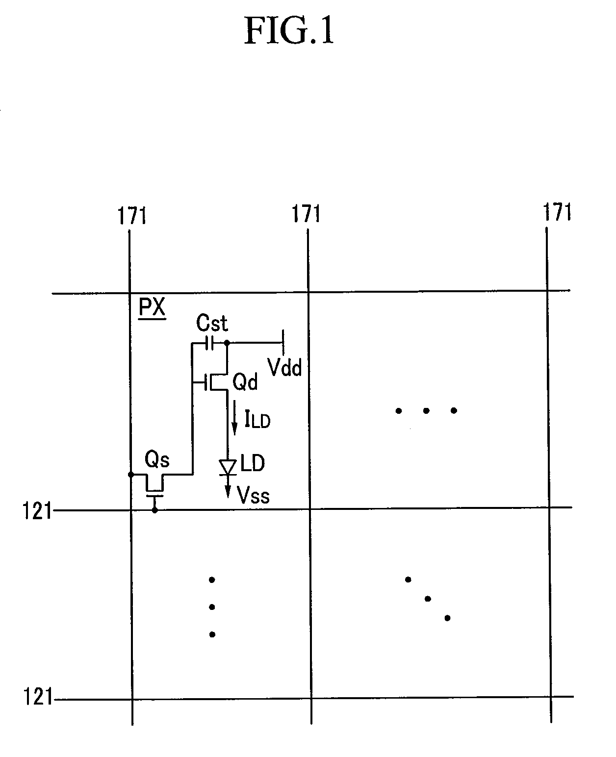
[0130]Now, an OLED display according to another exemplary embodiment of the present invention will be described in detail with reference to FIG. 15 and FIG. 16 as well as FIG. 1.

[0131]FIG. 15 is a layout view of an OLED display according to another exemplary embodiment of the present invention, and FIG. 16 is a cross-sectional view of the organic light emitting device shown in FIG. 15 taken along line XVI-XVI′-XVI″.

[0132]The present exemplary embodiment relates to an OLED display including a switching thin film transistor and a driving thin film transistor of a bottom gate structure, differently from the previous exemplary embodiment, and will now be described. Descriptions overlapping those of the previously described exemplary embodiment are omitted, and the same constituent elements are indicated by the same reference numerals.

[0133]A plurality of gate lines 121 including a plurality of switching control electrodes 124a and a plurality of driving control electrodes 124b are forme...

exemplary embodiment 3

[0146]Now, an OLED display according to another exemplary embodiment of the present invention will be described with reference to FIG. 17 and FIG. 18.

[0147]FIG. 17 is a layout view of an OLED display according to another exemplary embodiment of the present invention, and FIG. 18 is a cross-sectional view of the OLED display shown in FIG. 17 taken the line XVIII-XVIII.

[0148]The present exemplary embodiment further includes a driving voltage line parallel to a data line as well as a driving voltage line formed with the same layer as the pixel electrode, differently from the previous exemplary embodiment. Descriptions overlapping with the above-described exemplary embodiment are omitted, and the same constituent elements are indicated by the same reference numerals.

[0149]A plurality of gate lines 121 including a plurality of switching control electrodes 124a and a plurality of driving control electrodes 124b are formed on an insulating substrate 110, and a gate insulating layer 140 is ...


PUM


Abstract

The present invention relates to an OLED display and a manufacturing method thereof, including a gate line, a data line intersecting the gate line, a switching thin film transistor connected to the gate line and the data line, a driving thin film transistor connected to the switching thin film transistor, a first driving voltage line connected to the driving thin film transistor and overlapping the gate line and the data line, a first electrode connected to the driving thin film transistor, a second electrode facing the first electrode, and an light emitting member disposed between the first electrode and the second electrode.

Description

CROSS-REFERENCE TO RELATED APPLICATION[0001]This application claims priority under 35 U.S.C. §119 to Korean Patent Application No. 10-2007-0117379 filed in the Korean Intellectual Property Office on Nov. 16, 2007, the contents of which are incorporated herein by reference in their entirety.BACKGROUND OF THE INVENTION[0002](a) Field of the Invention[0003]The present invention relates to an organic light emitting device and a manufacturing method thereof.[0004](b) Description of the Related Art[0005]Trends toward lightweight and thin personal computers and televisions sets also require lightweight and thin display devices, and flat panel displays such as a liquid crystal display (LCD) satisfying such requirements are being substituted for conventional cathode ray tubes (CRTs).[0006]However, because the LCD is a passive display device, an additional back-light as a light source is needed, and the LCD has various problems such as a slow response time and a narrow viewing angle.[0007]Amo...

Claims


Application Information

Patent Timeline
IPC IPC(8): H01J1/62H01J9/20H05B44/00
CPCH01L27/1229H01L27/3276H01L27/1251H10K59/131G09G3/3233
Inventor LEE, BAEK-WOON
Owner SAMSUNG DISPLAY CO LTD
Why Eureka
Try Eureka