Transistor drive circuit of power converter operating in a wide voltage range

a technology of transistor drive and power converter, which is applied in the direction of logic circuit coupling/interface arrangement, pulse technique, instruments, etc., can solve the problems of low output voltage of switching signal vgb>2/b>, significant change at the supply voltage vsub>cc/sub>, and unlimited output voltage of switching signal vsub>g1/sub>

Active Publication Date: 2008-12-30
SEMICON COMPONENTS IND LLC
View PDF4 Cites 20 Cited by
  • Summary
  • Abstract
  • Description
  • Claims
  • Application Information

AI Technical Summary

Benefits of technology

[0012]An object of the present invention is to develop a transistor drive circuit of a power converter for operating in a wide voltage range. It includes an N-type high-side transistor, a P-type high-side transistor and an N-type low-side transistor. A voltage clamp device is connected to the gate of the N-type high-side transistor to limit the maximum output voltage of the N-type high-side transistor. The voltage level of the output signal through the P-type high-side transistor is the same as the supply voltage of the transistor drive circuit. However, a detection circuit is coupled to detect the supply voltage of the transistor drive circuit for generating a disable signal in response to the voltage level of the supply voltage. The disable signal is coupled to disable the P-type high-side transistor once the voltage level of the supply voltage is higher than a threshold voltage.

Problems solved by technology

However, the variation of the output voltage VO is wide once the power converter is operated in CC mode, which will cause a significant change at the supply voltage VCC.
The disadvantage of this circuit is an unlimited output voltage of the switching signal VG1.
The disadvantage of the circuit shown in FIG. 5 is a low output voltage of the switching signal VG2, particularly when the supply voltage VCC is low.
Furthermore, a low gate-to-source voltage will cause a high RDS-ON (drain-to-source ON resistance) of the transistor, which will increase the power losses of the power converter.
Both output drive circuits shown in FIG. 4 and FIG. 5 are inadequate to be used in a wide range of the supply voltage VCC.

Method used


Image

  • Transistor drive circuit of power converter operating in a wide voltage range
  • Transistor drive circuit of power converter operating in a wide voltage range
  • Transistor drive circuit of power converter operating in a wide voltage range

Examples


Embodiment Construction

[0021]Reference will now be made in detail to the present preferred embodiments of the invention, examples of which are illustrated in the accompanying drawings. Wherever possible, the same reference numbers are used in the drawings and the description to refer to the same or like parts.

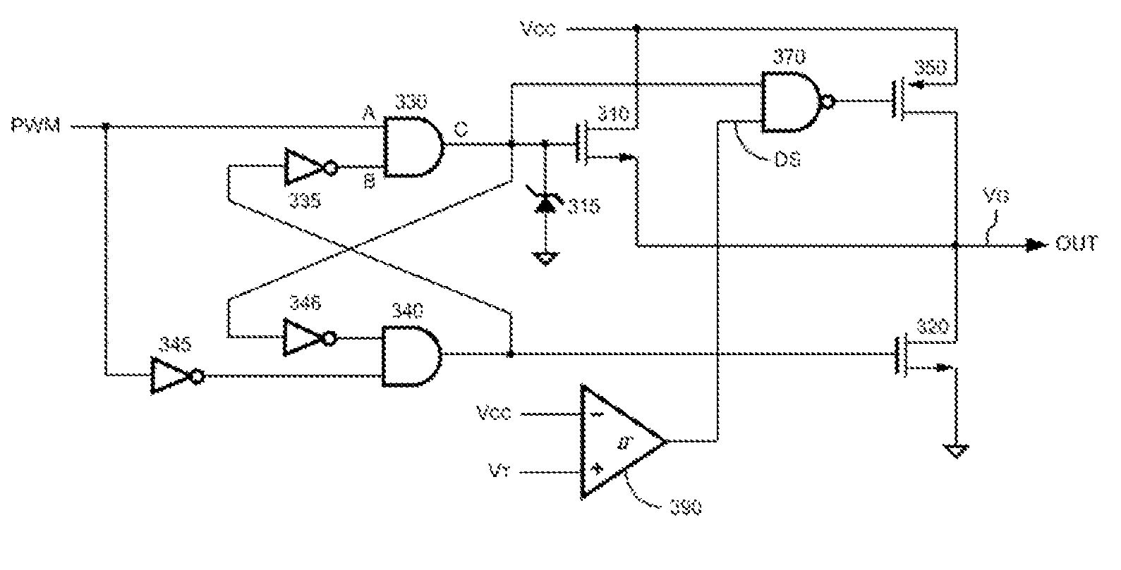
[0022]FIG. 7 shows a preferred transistor drive circuit according to the present invention. It includes an input terminal VCC to receive the supply voltage VCC. Several logic devices, such as AND gates 330 and 340, inverters 335, 345 and 346, an NAND gate 370, and an comparator 390, develop a control circuit. The output terminal OUT is coupled to output the switching signal VG for driving the transistor 20 of the power converter. A type-I transistor, which is the N-type high-side transistor 310 in the embodiment, having a drain terminal is coupled to the input terminal VCC. A source terminal of the N-type high-side transistor 310 is coupled to the output terminal OUT. A type-II transistor, which is t...


PUM


Abstract

A transistor drive circuit of a power converter is developed for operating in a wide voltage range. It includes an N-type high-side transistor, a P-type high-side transistor and an N-type low-side transistor. A voltage clamp device is connected to the gate of the N-type high-side transistor to limit the maximum output voltage. A detection circuit is coupled to detect the supply voltage of the transistor drive circuit to generate a disable signal in response to the voltage level of the supply voltage. The disable signal is coupled to disable the P-type high-side transistor once the voltage level of the supply voltage is higher than a threshold voltage.

Description

BACKGROUND OF THE INVENTION[0001]1. Field of Invention[0002]The present invention relates to a transistor drive circuit, and more specifically relates to a transistor drive circuit of a power converter.[0003]2. Description of Related Art[0004]Power converters have been widely used to provide regulated power supplies for computers, home appliances, communication equipments, mobile phones, etc. FIG. 1 shows a power converter for a battery charger. The maximum output voltage and the maximum output current of the power converter are regulated. It includes a transformer 10 having a primary winding NP, a secondary winding NS and an auxiliary winding NA. One terminal of the primary winding NP is coupled to an input voltage VIN. Another terminal of the primary winding NP is connected to a transistor 20. The transistor 20 is applied to switch the transformer 10 and regulate the output of the power converter. A switching control circuit 100 is coupled to the output of the power converter thro...

Claims


Application Information

Patent Timeline
Patent Type & Authority Patents(United States)
IPC IPC(8): H03K3/00
CPCH02M1/08H02M3/335H03K17/08122H03K17/162H03K17/22H03K17/6871
Inventor YANG, TA-YUNGTSAO, FENG-CHENGLI, CHUH-CHINGWANG, JESSE R.
Owner SEMICON COMPONENTS IND LLC
Why Eureka
Try Eureka