Method and apparatus for bump inspection

a three-dimensional inspection and apparatus technology, applied in the direction of measurement devices, material analysis through optical means, instruments, etc., can solve the problems of component failure, add to total production time, and not be suitable for inspecting every component, so as to reduce the distortion of perspective

Inactive Publication Date: 2008-12-30
AGENCY FOR SCI TECH & RES
View PDF6 Cites 4 Cited by
  • Summary
  • Abstract
  • Description
  • Claims
  • Application Information

AI Technical Summary

Benefits of technology

[0011]The imaging device may include a telecentric lens for reducing perspective distortion, and may be selected from the group consisting of: a colour CCD camera and a black and white CCD camera.
[0020]The imaging device may include a telecentric lens for reducing perspective distortion, and may be selected from the group consisting of: a colour CCD camera and a black and white CCD camera.

Problems solved by technology

Wafer bump and / or solder ball height and coplanarity inspections are commonly carried out to check for any significant unevenness and missing bumps or balls, because such defects in a component mean loss of electrical contact, leading to component failure.
Such methods are not suitable for inspecting every component produced as they need the component to be stopped momentarily for image capturing —adding to total production time and hence increasing production costs.
Since only a sample group of each production batch will be inspected, defective components will still get passed if they do not happen to be in the sample group.
Side view images captured by such methods are also limited in depth of view, requiring multiple exposures to be made in order to inspect the whole component if the component size is greater than the depth of view.
Again, this increases inspection time.

Method used


Image

  • Method and apparatus for bump inspection
  • Method and apparatus for bump inspection
  • Method and apparatus for bump inspection

Examples


Embodiment Construction

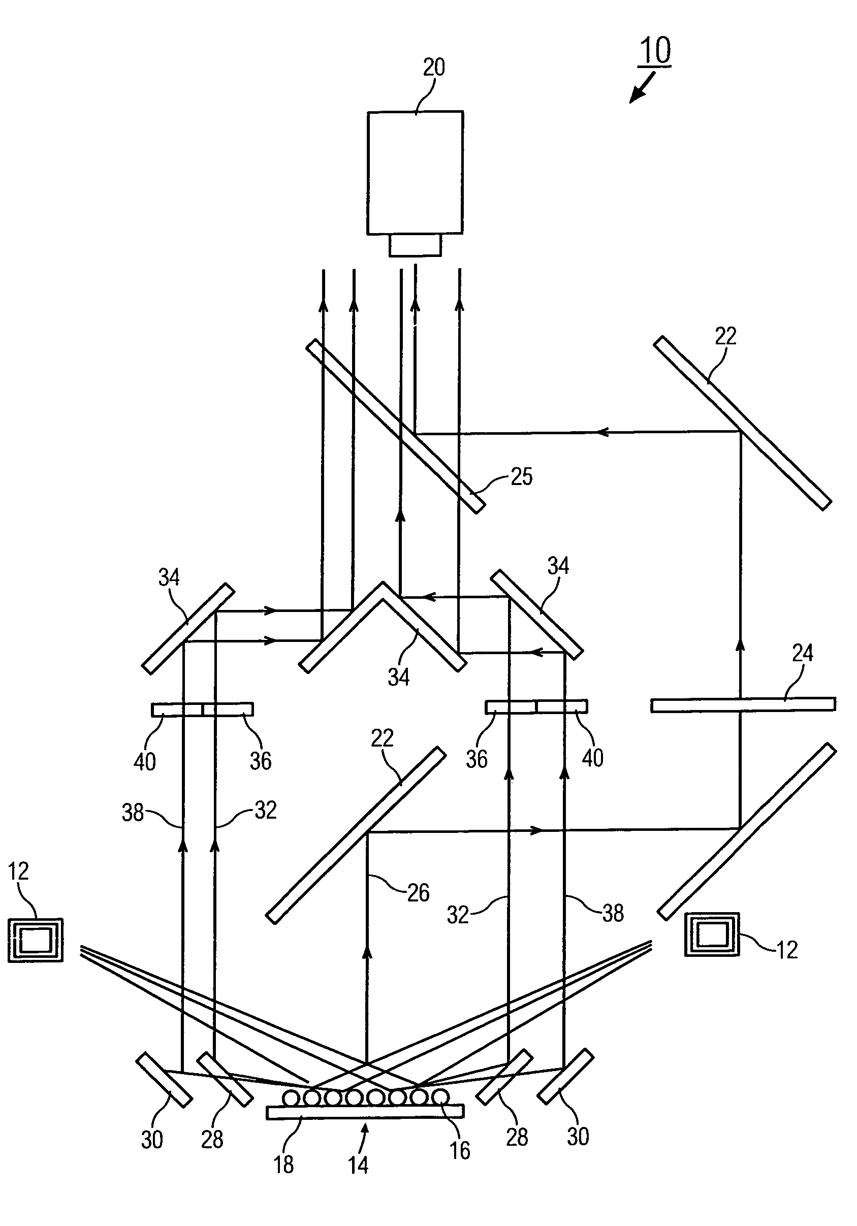
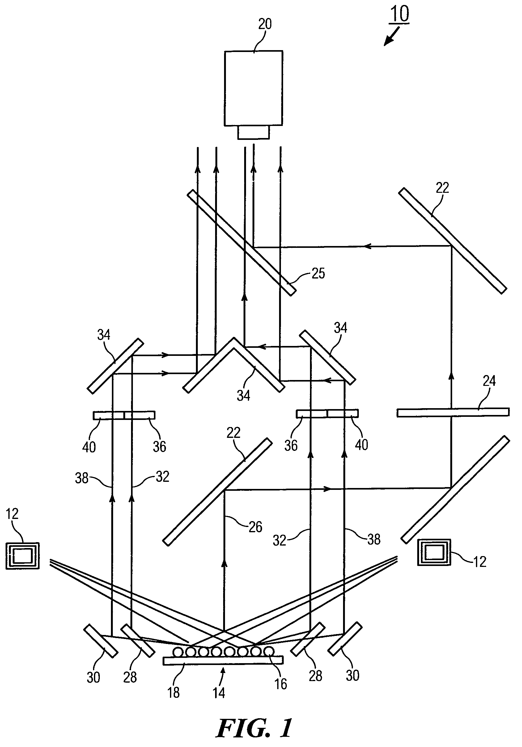
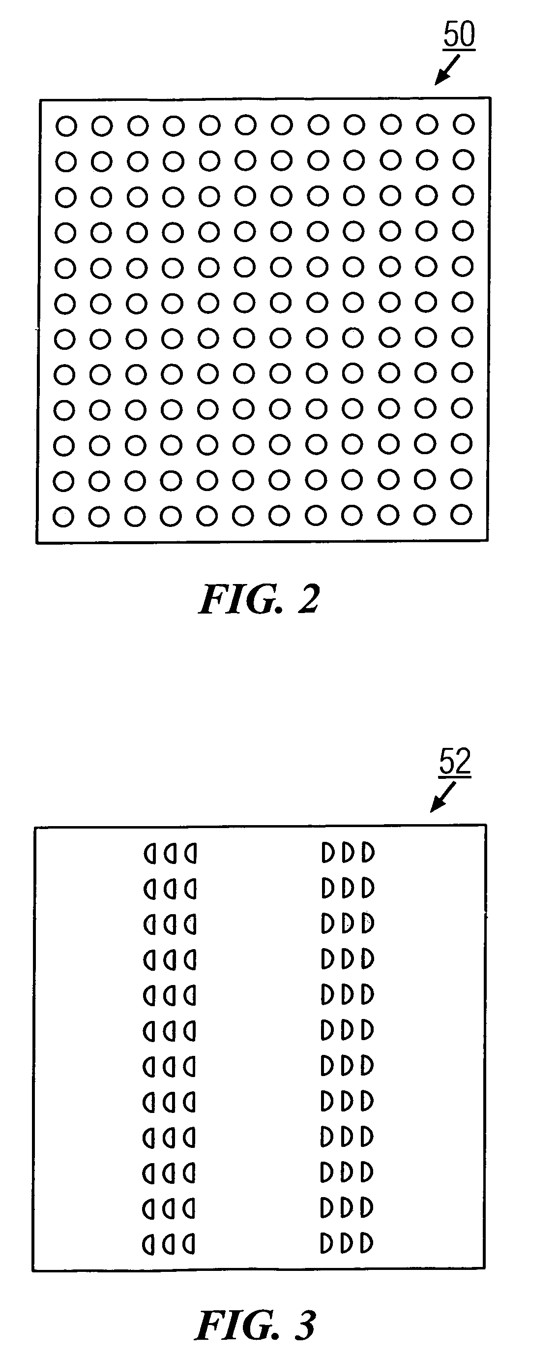
[0036]According to one aspect, there is provided an apparatus 10 for dynamic three-dimensional inspection of bumps as shown in FIG. 1. The apparatus 10 comprises at least one colour light source 12 for illuminating a component 14 having a plurality of bumps 16 disposed on a surface 18. The component 14 can be for example a wafer bump or ball grid array (BGA) device. The colour light source 12 may be an LED light, a halogen light or other triggerable light source. Preferably, the colour light source 12 comprises red, green and blue light emitting diodes (LEDs) for providing light of respective wavelengths of 50% point at 580 nm, 485 nm and 475 nm, and has separate brightness control for light of each wavelength. Multispectral light comprising a plurality of different wavelengths (e.g. red, green and blue light) from the light source 12 is projected onto the plurality of bumps 16 at a low oblique angle, incident at preferably between 10° to 25° from the surface 18.

[0037]The apparatus ...


PUM

PropertyMeasurementUnit
angleaaaaaaaaaa
angleaaaaaaaaaa
angleaaaaaaaaaa

Abstract

A method of dynamically imaging, calibrating and measuring bump height and coplanarity of a plurality of bumps on a surface is disclosed. The method includes illuminating the plurality of bumps with multispectral light from at least one light source, and receiving light of a first wavelength at an imaging device such that a top view image of at least a portion of the plurality of bumps is captured. The light of the first wavelength is reflected off the plurality of bumps at a first angle from the surface. Light of a second wavelength is received at the imaging device such that at least one oblique side view image of at least a portion of the plurality of bumps is captured. The light of the second wavelength is reflected off the plurality of bumps at a second angle from the surface. The captured images are processed to determine absolute bump height and coplanarity. A corresponding apparatus is also disclosed.

Description

FIELD OF THE INVENTION[0001]This invention relates to a method and apparatus for three dimensional inspection of bumps, and particularly, but not exclusively, to dynamic inspection of moving wafer bumps and ball grid arrays.DEFINITION[0002]Bump is taken to include a wafer bump and a solder ball in a ball grid array.BACKGROUND OF THE INVENTION[0003]Wafer bump and / or solder ball height and coplanarity inspections are commonly carried out to check for any significant unevenness and missing bumps or balls, because such defects in a component mean loss of electrical contact, leading to component failure.[0004]Current methods include taking multiple images of a plurality of bumps on a surface of a component from different viewpoints and angles, and performing triangulation calculations on related measurements of the images to determine a three dimensional position of each bump with reference to a pre-calculated calibration plane. This is achieved by holding the component stationary while ...

Claims


Application Information

Patent Timeline
Patent Type & Authority Patents(United States)
IPC IPC(8): G01N21/00
CPCG01B11/0608G01B11/306
Inventor XU, JIANLIU, TONG
Owner AGENCY FOR SCI TECH & RES
Why Eureka
Try Eureka