Method of matching layout shapes patterns in an integrated circuit using walsh patterns

a technology of layout shapes and integrated circuits, applied in the field of design automation, can solve problems such as the difficulty of yield characterization engineers, systematic defects relating to shapes layout design flaws or processing design flaws, and the defect of systematic defects in a semiconductor process, so as to reduce false positives

Inactive Publication Date: 2008-12-30
GLOBALFOUNDRIES INC
View PDF5 Cites 1 Cited by
  • Summary
  • Abstract
  • Description
  • Claims
  • Application Information

AI Technical Summary

Benefits of technology

[0015]Accordingly, it is an object of the invention to reduce false positives in pattern matching by using an orthogonal sub-space projection of layout shapes using Walsh patterns.
[0016]It is another object of the invention to separate the density extraction from the projection, allowing overlapping windows for high resolution search and allowing density data to be reused for other target window sizes.
[0018]These and other objects of the invention are provided by a pattern matching system for layout shapes using Walsh patterns. The invention reduces false positives in pattern matching in comparison to the prior art method. The invention enables the same density data to be reused as a window is stepped in small increments across the layout, whereas the prior art method prevented density data from being reused. The invention also enables the same density data to be reused for other target window sizes. Any subset of Walsh patterns is covered and the invention is not limited to having the Walsh pattern resolution be the same as the layout window resolution.

Problems solved by technology

Systematic defects in a semiconductor process are defects which are not a result of particles interfering with exposure or other lithographic process steps during manufacturing.
Instead, systematic defects relate to shapes layout design flaws or processing design flaws and which occur regularly at the same location within a finished product.
Yield characterization engineers face a difficult task when trying to identify the root cause of such defects.
Particularly, in modern processes requiring resolution enhancement, chemo-mechanical polishing and other complex steps, the root cause often involves the interaction of a particular local pattern with the shapes within its context.
The same pattern which results in a deterministic fail or is not robust to process variations in a particular part number may not fail in other locations on the same design, or on a different design.
However, the prior art intersection method is not an orthogonal projection.
The problem with the non-orthogonal projection system is that data loss occurs.
The feature resolution is poor, resulting in excessive false positives.
In addition to excessive false positives, the prior art intersection method precludes reusing density values.
Therefore, there is no way by which one may achieve a higher resolution search using the prior art method of image recognition.
Inability to achieve a higher resolution search results in missed matches.

Method used


Image

  • Method of matching layout shapes patterns in an integrated circuit using walsh patterns
  • Method of matching layout shapes patterns in an integrated circuit using walsh patterns
  • Method of matching layout shapes patterns in an integrated circuit using walsh patterns

Examples


Embodiment Construction

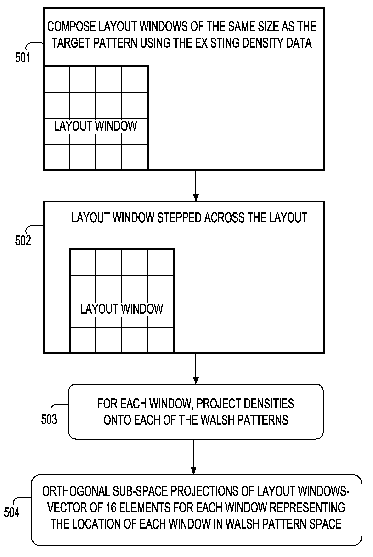
[0027]The present invention and the various features and advantageous details thereof are explained more fully with reference to the non-limiting embodiments that are illustrated in the accompanying drawings and detailed in the following description.

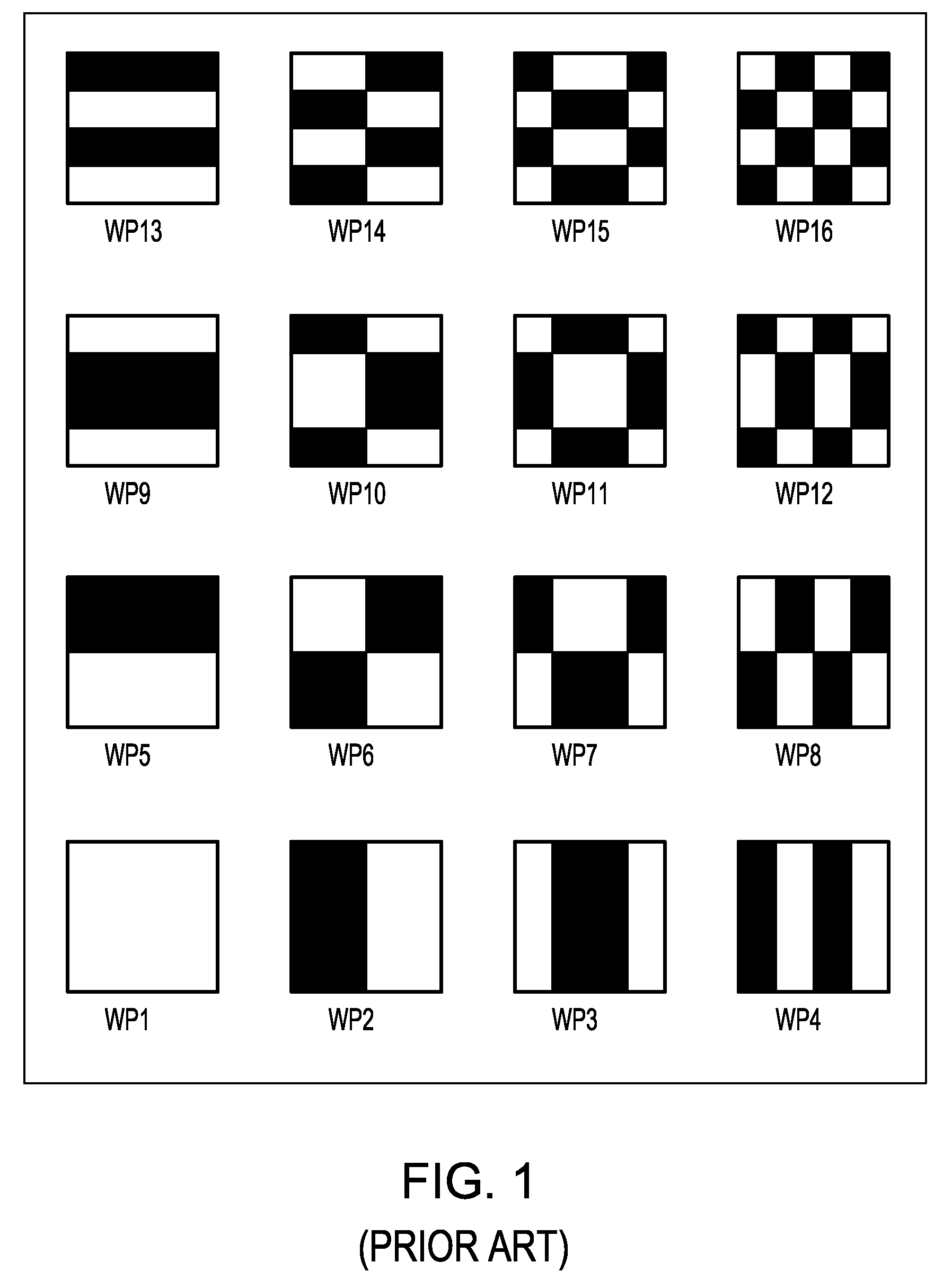
[0028]Referring to FIG. 1, a set of typical Walsh patterns is selected. As would be readily understood by one ordinarily skilled in the art, the choice of 16 is merely an example and any orthogonal set of Walsh patterns may be used.

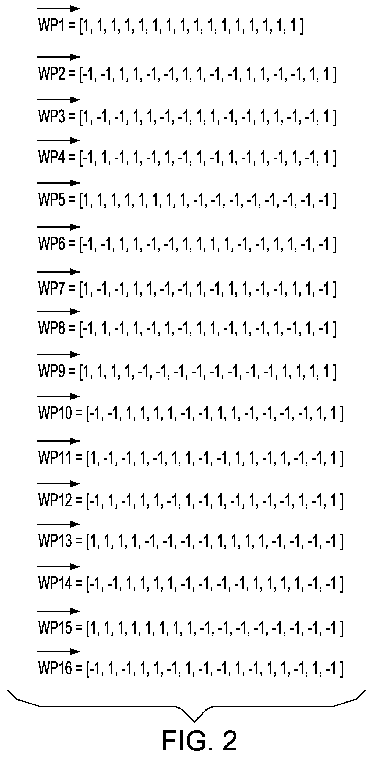
[0029]Referring to FIG. 2, the Walsh patterns define basis vectors which form the feature space. In the example illustrated, the feature space is 16-dimensional. The conversion process from a Walsh pattern to the corresponding basis vectors shown in FIG. 2 is as follows. Each Walsh pattern is divided into 16 rectangles (4 rows and 4 columns). Beginning with the bottom row and the lower left corner of the image and progressing from left to right for each row, a +1 is used for each black rectangle and −1 for eac...


PUM


Abstract

A method for matching patterns, based on an orthogonal sub-space projection of layout shapes using Walsh patterns, performs a preliminary density feature extraction of a circuit design layout, allows a user to define a pattern, and performs a high resolution search of the layout to locate all instances of the pattern. A sorted list of layout windows ranging from the most similar to quantitatively less similar is generated. The method for matching patterns significantly reduces false positives in comparison with the prior art and enables the same density data to be reused as a window is stepped in small increments across the layout.

Description

FIELD OF THE INVENTION[0001]The present invention generally relates to the field of Design Automation, and more particularly, to a method for matching layout shapes patterns in a larger integrated circuit shapes layout for the purpose of performing a systematic defect analysis.DESCRIPTION OF RELATED ART[0002]Systematic defects in a semiconductor process are defects which are not a result of particles interfering with exposure or other lithographic process steps during manufacturing. Instead, systematic defects relate to shapes layout design flaws or processing design flaws and which occur regularly at the same location within a finished product. Yield characterization engineers face a difficult task when trying to identify the root cause of such defects. Particularly, in modern processes requiring resolution enhancement, chemo-mechanical polishing and other complex steps, the root cause often involves the interaction of a particular local pattern with the shapes within its context.[...

Claims


Application Information

Patent Timeline
Patent Type & Authority Patents(United States)
IPC IPC(8): G06F17/50G06V10/50
CPCG06F17/5081G06K9/4642G06F30/398G06V10/50
Inventor LEHNER, VALERIE D.LEHNER, TIMOTHY S.
Owner GLOBALFOUNDRIES INC
Why Eureka
Try Eureka